
An Aluminum Nitride PCB inverter module release should connect panel handling, copper interfaces, and inspection evidence before production volume is authorized.
Inverter modules expose the difference between a ceramic concept and a repeatable production process. Heavy copper, AlN substrate, switching devices, isolation clearances, carrier support, and inspection access all compete for the same panel area. A drawing that only states pad and hole dimensions leaves the supplier to guess about edge handling, tooling, bond sequence, and the evidence needed for release. The project needs a DFM package that is specific about risk without pretending every result is already measured.
Make the panel carry the process intent
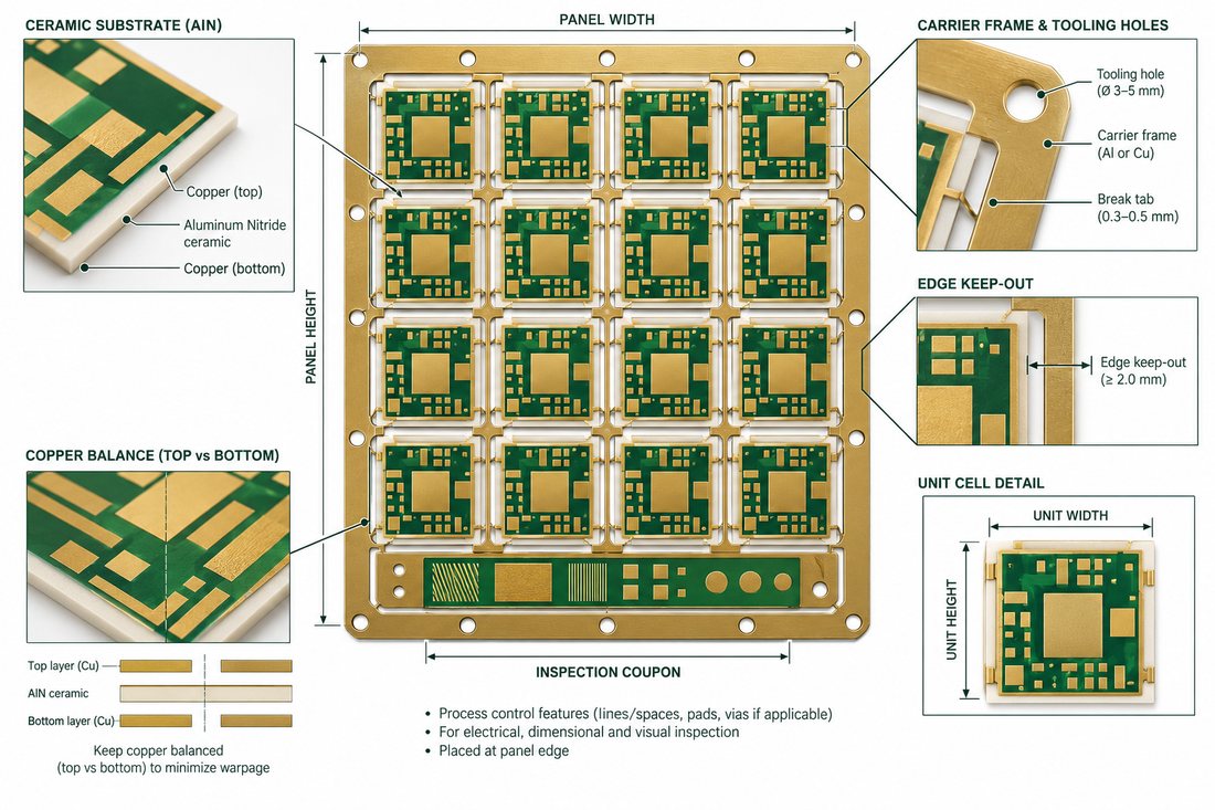
Show the array, support rails, tooling holes, breakaway method, copper balance, and coupon locations. The Aluminum Nitride PCB panel should keep heavy-copper edges supported and leave an inspection route for the device pads, backside interface, and isolation features.
Define the finished thickness, copper construction, bond or attach method, surface finish, and approved alternate material. The thermal management manufacturing review should mark edge keep-outs, carrier contact, and any area where a fixture may load the ceramic.
Panel design is an electrical decision when copper density changes the current path or thermal spreader. Recheck the power loop and RF or gate return after a panel ECO.
Align assembly and inspection evidence
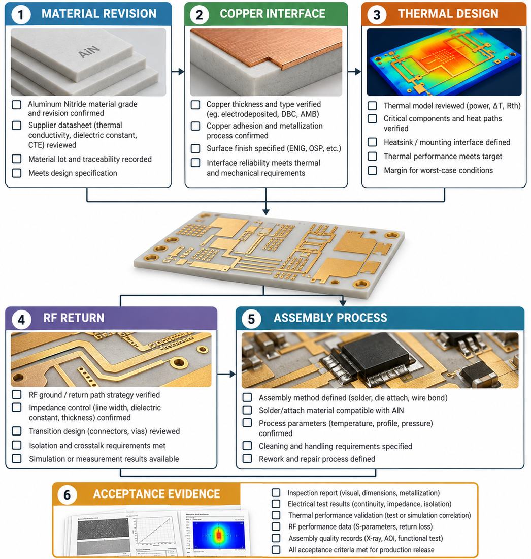
The assembly package should include placement datums, paste or braze condition, support points, reflow or firing window, cleaning, and coplanarity criteria. The Aluminum Nitride PCB acceptance plan should name the sample, method, and record returned for each lot.
Use cross-sections and continuity checks at the product features that drive risk. A witness coupon is useful only when it shares the material, copper, and thermal history. The RF PCB quality record should state that relationship rather than treating a coupon as universal proof.
Protect heavy copper and ceramic edges during depanelization and packing. A cosmetic chip may be rejectable when it reaches an isolation edge or a connector datum.
Control procurement and ECO decisions
Keep material revision, copper interface, panel, assembly drawing, and inspection plan synchronized. The controlled impedance procurement note should require engineering approval for any substitute that changes dielectric, thermal, CTE, or metallization behavior.
When an ECO moves a pad, edge, device, or tooling hole, repeat the affected DFM and thermal checks. Do not approve a “layout-only” change if it alters support or measurement access.
Close with a release checklist covering material, copper, panel, assembly, inspection, packaging, approved alternates, and deviation ownership. That is the handoff procurement and quality can act on.
Aluminum Nitride PCB inverter production is controlled by the panel and handoff as much as by the substrate. Put process intent, inspection evidence, and change ownership into the release before the volume order.
For project control, record the interface owner, drawing revision, supplier capability note, and the exact condition that would reopen the review. A clear decision log is especially useful when a sourcing change, enclosure change, or assembly change arrives after the RF model has been signed off. The team can then distinguish a harmless documentation update from a change that requires a new coupon, cross-section, or environmental check.
Engineering release note: keep the thermal interface, RF reference, and inspection datum visible in the same revision-controlled package. When a device, copper feature, carrier, or assembly step changes, identify the affected assumption and repeat only the evidence tied to that boundary. This prevents a typical material value from being mistaken for a guaranteed product result.
Release note: keep the Aluminum Nitride PCB panelization, handling method, and release checklist aligned before an inverter module enters volume production.
Sources: CeramTec aluminum nitride substrate data; Analog Devices RF and mixed-signal PCB layout guidance; supplier application notes for direct-bond copper and high-power ceramic modules. Numerical values are treated as typical supplier values, design targets, or engineering ranges unless a released drawing defines a measured acceptance value.
Release gate: document the Aluminum Nitride PCB interface before approval.
Release gate: document the Aluminum Nitride PCB interface before approval.
Release gate: document the Aluminum Nitride PCB interface before approval.
Release gate: return the PCB manufacturing evidence with the lot package.
Release gate: return the PCB assembly evidence with the lot package.
