
A Smart Home PCB may be electrically correct and still lose yield when it is released as a panel. Sensor vents, tooling rails, fiducials, connector edges, and coating masks all compete for the same millimeters. The release decision is not simply “can the board be routed?” It is whether the panel can be assembled, separated, coated, inspected, and packed without changing the sensor interface or radio keep-out. This guide turns those project risks into a practical panel and finish definition.
- Choose a panel orientation that protects the sensor port and connector edge.
- Balance copper and tooling features before approving the array.
- Separate coating masks from assembly and test access.
- Keep first-article evidence tied to the same panel revision.
Panelize around the sensor and the operator datum
The sensor opening is often the first feature damaged by a careless route or V-score. A Smart Home PCB panel should place the environmental port away from breakaway tabs and support rails. If the sensor must remain open during coating or calibration, mark a no-touch zone on the panel drawing, not only in a 3D enclosure model. A repeated board-to-board orientation also makes operator loading and camera inspection less ambiguous.
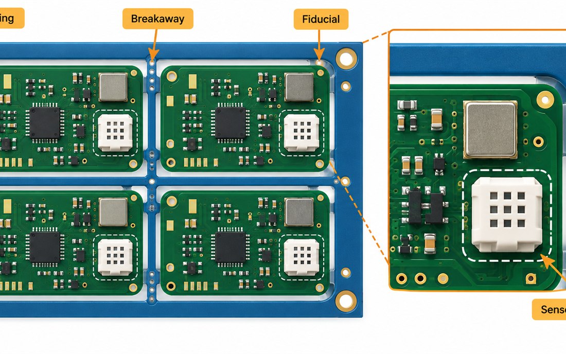
Use the PCB design database to carry the panel outline, fiducial strategy, and component height limits. A panel that looks efficient on a spreadsheet may put a connector over a support pin or force a nozzle to approach the sensor from the wrong direction. The project manager should ask for the operator loading direction and the first-article photo before approving the final array.
Balance copper before the first assembly build
Large ground pours, battery planes, and shield areas can pull heat differently from a mostly empty sensor corner. The PCB materials stackup, copper weight, and solder-mask opening should be reviewed with the panel rails. If the panel is asymmetric, a board can bow during reflow even though its individual outline is within drawing limits. Treat copper balance as a process input, not an afterthought for the PCB manufacturing quote.
Keep assembly, test, and coating access separate
A connector clearance needed by a pick-and-place nozzle is not the same as the clearance needed by a test probe or a coating mask. Mark these interfaces as separate layers in the release drawing. The PCB assembly team needs component keep-outs and support locations; the test team needs probe access and a stable datum; the coating team needs a mask boundary and a cure or inspection path.
| Panel feature | Failure if omitted | Release evidence |
|---|---|---|
| Tooling holes | Fixture shift or uneven support | Panel drawing and first-article fit |
| Fiducials | Placement offset or camera ambiguity | Assembly inspection record |
| Sensor mask | Blocked port or changed response | Mask artwork and inspection photo |
| Breakaway relief | Stress at connector or sensor corner | Depanelization review |
For a PCB assembly revision, identify whether the mask belongs to a component body, a port, or a test pad. Mixing those categories creates an operator instruction that is difficult to audit. A controlled RF PCB return path may also need a keep-out from a depanelization tool, because a nicked ground edge can affect both EMC behavior and mechanical fit.
Selective coating is a drawing problem before it is a chemistry problem
Conformal coating protects a smart-home node from condensation and contaminants, but coating the wrong surface can block a sensor vent, trap solvent, or insulate a connector contact. The PCB material, solder mask, and coating system must be named together. If a substitute coating is allowed, record its cure condition and the surfaces that must remain clear.
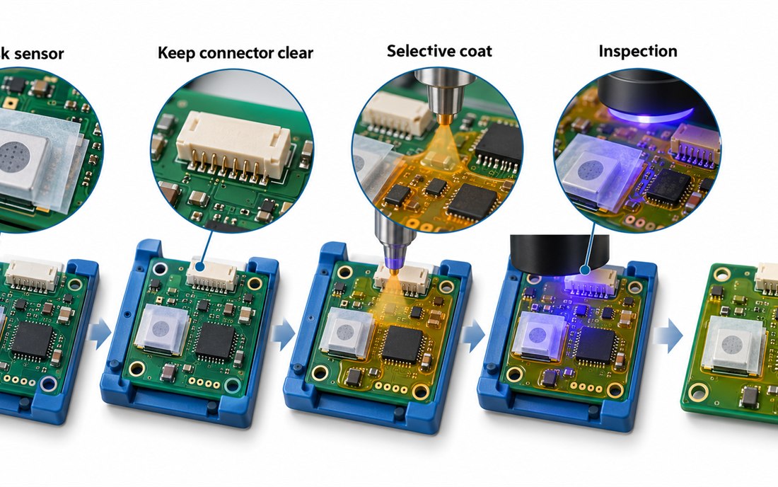
The mask boundary belongs in the manufacturing package, not in an informal email. Use a drawing layer or a marked-up assembly file to show the sensor port, connector contacts, programming pads, and current-shunt access. A clear PCB fabrication note prevents a line operator from interpreting a shaded copper area as a coating limit.
Release a panel with a traceable traveler
Smart Home PCB fabrication depends on the approved laminate family, and the Smart Home PCB review must preserve the same sensor datum. The Smart Home PCB traveler then ties the panel and finish to production evidence.
The traveler should identify panel revision, board orientation, tooling holes, approved material family, assembly program, coating recipe, and inspection method. The DFM review sign-off is incomplete if it does not state how the board is separated and how the sensor port is protected afterward. Keep the same board identifier on the panel drawing, fixture record, and serialized calibration result.
- Confirm the panel image matches the released Gerber and drill files.
- Check that sensor and connector masks remain visible after the assembly step.
- Inspect depanelized edges near RF returns, mounting holes, and sensor ports.
- Record coating lot and inspection revision with the board lot.
- Repeat the fit check after any rail, tab, or enclosure ECO.
A production-ready Smart Home PCB panel is a coordinated mechanical and electrical interface. When tooling, copper balance, coating masks, and calibration access are specified together, a change to one fixture or enclosure does not silently turn into a field reliability problem.
Procurement should approve only the approved PCB material, assembly finish, and panel process that the traveler can identify. That gives engineering a defensible change-control record and gives the line a repeatable way to build the next lot.
Panel change control for a Smart Home PCB
When a Smart Home PCB moves from a prototype outline to a production panel, the Smart Home PCB owner should compare the rail, fiducial, breakaway, and sensor-port notes. A Smart Home PCB coating mask is part of the same release as the assembly drawing. If the Smart Home PCB connector changes, the panel support and inspection view must be rechecked. The Smart Home PCB traveler should identify the material, finish, and serialized board lot so a later Smart Home PCB complaint can be traced to a panel revision rather than guessed from a photograph.
Sources: Würth Elektronik assembly and EMC notes; Analog Devices sensor and mixed-signal layout guidance; Qorvo RF integration references; coating, connector, stencil, and PCB material supplier application data. The checks above are engineering release practices, not customer test results.
