HomeTag

Copper Balance - KKPCB

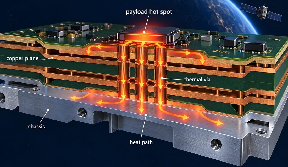
Satellite PCB Thermal Drift: Managing CTE, Copper Density, and Chassis Interfaces

Satellite PCB thermal drift becomes a mission risk when a board is treated as a flat electrical drawing instead of a constrained mechanical and thermal assembly. A payload can meet its schematic targets and still show connector strain, oscillator frequency movement, or intermittent solder fatigue after repeated hot-cold transitions. This Satellite PCB thermal drift problem...
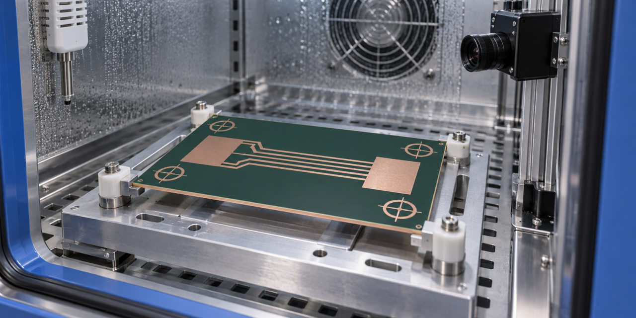
RO5880 PCB Dimensional Stability: Managing Moisture and Registration in Outdoor Radar

Outdoor radar and microwave equipment can see humidity, temperature swings, and repeated handling before a board reaches final system test. For a PTFE-based laminate, the project risk is not only RF loss; it is whether the finished RO5880 PCB keeps its layer registration, connector datum, and antenna geometry through the approved process. This RO5880 PCB...

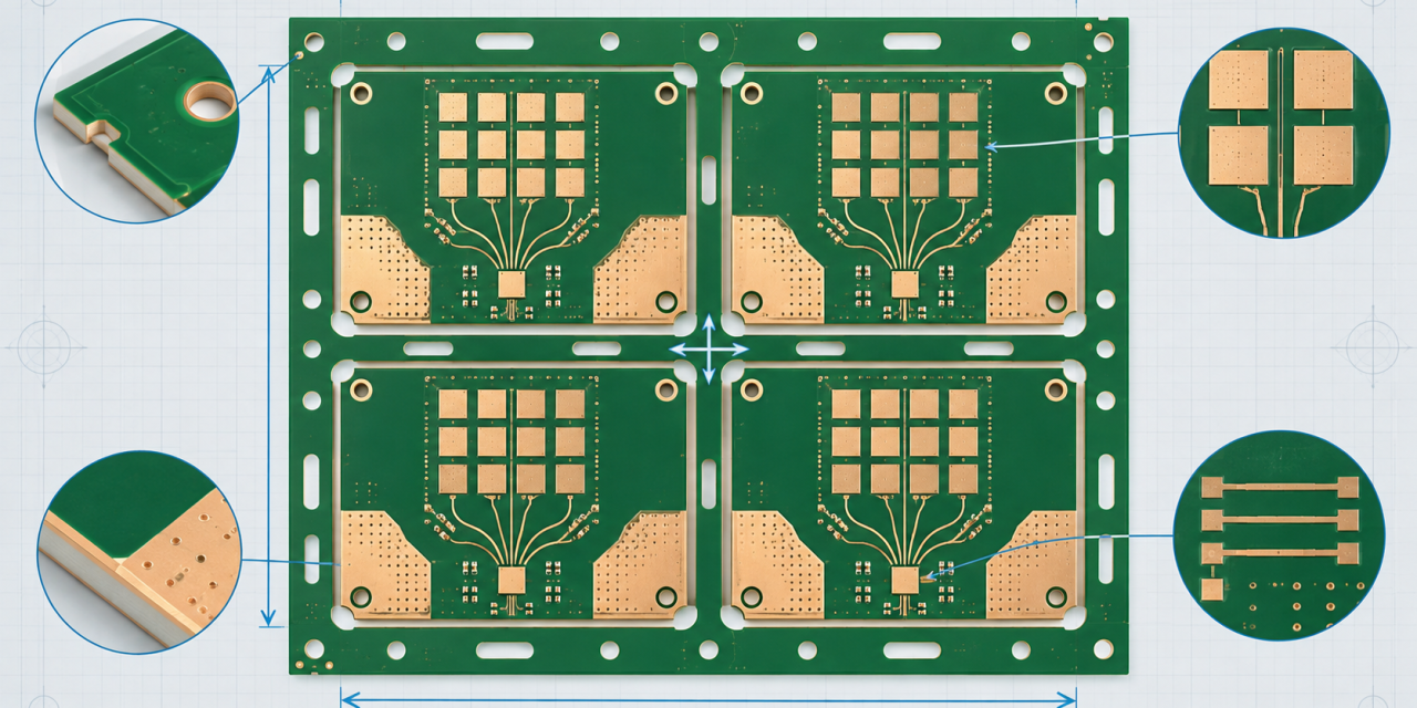
RO4003C PCB Panelization for 5G Antenna Arrays: Controlling Phase Consistency and RF Yield

When a 5G antenna array moves from prototype to volume production, the difficult question is rarely whether the RF layout works once. The risk is whether every unit on a panel keeps the same phase center, launch geometry, and return-current path after imaging, lamination, plating, routing, and singulation. A disciplined RO4003C PCB panelization plan makes...

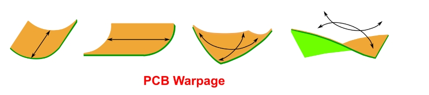
What is PCB warpage?

What is PCB Warpage? PCB warpage refers to the unwanted bending, twisting, or deformation of a printed circuit board from its intended flat shape. Ideally, a PCB should maintain a flat and stable surface throughout fabrication, assembly, and operation. However, differences in material properties, thermal expansion, copper distribution, and manufacturing processes can cause the PCB...