
When a 5G antenna array moves from prototype to volume production, the difficult question is rarely whether the RF layout works once. The risk is whether every unit on a panel keeps the same phase center, launch geometry, and return-current path after imaging, lamination, plating, routing, and singulation. A disciplined RO4003C PCB panelization plan makes those variables visible before the first production lot. For project teams, the RO4003C PCB release should include the panel drawing and its RF acceptance logic together.
Why array panelization changes RF behavior
Array elements share a common electromagnetic reference, so small differences in copper density, edge distance, dielectric thickness, or routing direction can become element-to-element phase error. A panel that is mechanically efficient but electrically asymmetric can create a repeatability problem that is difficult to isolate at system test. The panel drawing should therefore be treated as part of the 5G antenna array design, not as a late manufacturing convenience. This keeps the RO4003C PCB electrical frame visible to both layout and production teams.
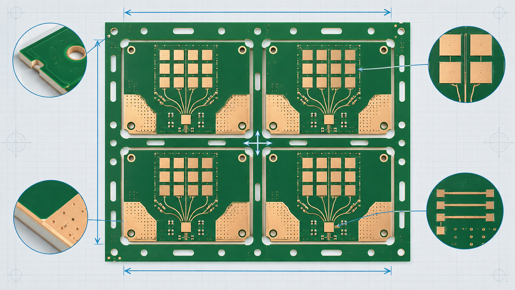
Start with a repeatable RO4003C PCB electrical frame
Place the RF apertures, feed transitions, and reference planes in the same orientation on every array position. Keep identical feed lines on the same panel axis whenever possible. This reduces the number of process variables that can be confused with a design variable. For a new RO4003C PCB stackup, use the design Dk recommended by the laminate supplier for initial field-solver work, then release the final impedance target with the fabricator after resin content, copper roughness, and finished dielectric thickness are known.
RO4003C PCB panelization for phase consistency
RO4003C PCB panelization is most repeatable when each array position shares one electrical datum and one documented manufacturing orientation.
Panel rails, tooling holes, and fiducials should not force an RF board close to a mechanically weak edge. Keep the antenna perimeter and connector launch away from rout paths and breakaway tabs. When the outline cannot be symmetric, mirror the electrical orientation in the CAD panel and flag the exception in the manufacturing drawing. That simple rule gives the process engineer a clear way to compare center, corner, and edge positions without claiming that all locations are identical by default.
| Panel feature | Engineering risk | Release control |
|---|---|---|
| Repeated array orientation | Element phase and polarity can vary by position | Lock one master datum and document any mirrored copy |
| Copper distribution | Uneven etch and lamination movement | Use copper-balance zones outside RF keep-outs |
| Rails and tooling | Edge stress or poor registration | Reserve a stable rail with verified tooling holes |
| RF coupons | Process drift is invisible without a witness | Place coupons in representative panel locations |
Manage copper balance without loading the RF aperture
Balanced copper is useful for etch and lamination stability, but dummy copper must not sit beneath an antenna aperture or beside a sensitive feed without an electromagnetic review. A manufacturing panel can use non-functional fill in mechanical margins while preserving a controlled keep-out around radiating features. For a mixed RF and digital design, define the RF stackup and RO4003C PCB copper-fill rules together so that the fabricator does not optimize one layer at the expense of another.
Translate the panel plan into DFM checkpoints
Before release, compare the individual RO4003C PCB board drawing with the array panel in three views: finished copper, drill and route, and fabrication notes. Check that every controlled-impedance line keeps its reference plane after tab routing and that plated-through holes do not create an unplanned stub. On multilayer constructions, confirm that the panelized drill table still maps to the same layer pairs. If the design uses fine-pitch transitions, a small HDI PCB substructure may be practical, but its microvia and capture-pad rules must be panel-qualified rather than copied from a different material family.
At this stage, the controlled impedance definition should include the reference plane, finished copper assumption, line-width tolerance, and the coupon location. Avoid a single nominal width with no process window. The goal is a measurable acceptance plan, not a promise that one calculated number will survive every fabrication step unchanged.
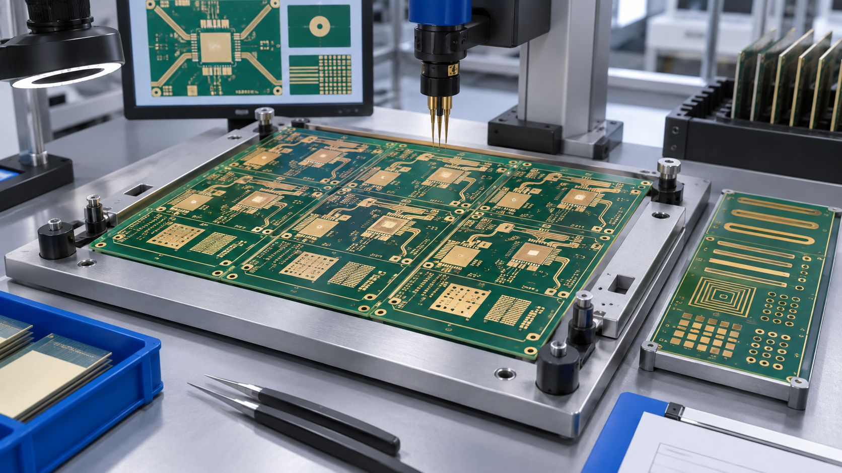
Use coupons to separate design issues from process issues
A coupon is most useful when its geometry represents the finished board: the same layer pair, copper weight, line style, and nearby plane structure. Put at least one coupon near the center and one near an edge when the panel has a large aspect ratio. Record panel ID, lot, stackup revision, and surface-finish route with the coupon result. These records help the team decide whether a failed RO4003C PCB antenna element is a layout problem, a registration shift, or a process excursion.
Release checklist for a production-ready panel
- Lock the master datum, board orientation, and any mirrored copies.
- Show rails, tooling holes, fiducials, breakaway method, and edge keep-outs.
- Review copper balance and RF keep-outs on every copper layer.
- Map impedance coupons to the stackup and finished-copper assumptions.
- Define inspection points for registration, plating, solder mask clearance, and routing.
- Record the approved material, revision, and panel drawing together in the release package.
KKPCB can review an RO4003C PCB panel drawing for PCB manufacturing risk before tooling is ordered. The review is most effective when the RF designer supplies the intended frequency band, array symmetry requirement, controlled-impedance table, and the acceptable distinction between a target value and a measured value.
Key takeaway
A reliable RO4003C PCB panel is an electrical repeatability tool as much as a production fixture. When a RO4003C PCB panel moves into volume, the same datum and coupon rules keep yield data comparable. By fixing the electrical frame, balancing copper outside RF keep-outs, and placing representative coupons, a 5G team can reduce phase-consistency surprises and make yield discussions evidence-based. The same logic applies when a panel moves from prototype quantity to a higher-volume build: preserve the datum and stackup intent first, then optimize panel utilization.
Sources: Rogers Corporation RO4000 series laminate data sheet and RO4003C product information; IPC-TM-650 impedance and dimensional test methods; KKPCB internal PCB design-for-manufacturing capability notes. Numerical values are typical material or design references, not customer measured results.
