
What is PCB Warpage?
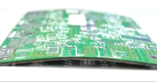
PCB warpage refers to the unwanted bending, twisting, or deformation of a printed circuit board from its intended flat shape. Ideally, a PCB should maintain a flat and stable surface throughout fabrication, assembly, and operation. However, differences in material properties, thermal expansion, copper distribution, and manufacturing processes can cause the PCB to become curved or uneven.
PCB warpage is especially critical in high-density PCB assemblies, multilayer boards, HDI boards, rigid-flex PCBs, and products requiring precise SMT placement. Excessive warpage can lead to assembly defects, reduced reliability, and difficulties during automated production.
Common Types of PCB Warpage
PCB warpage is generally classified into several forms:
1. Bow
Bow is a smooth, continuous curvature where the entire PCB bends along one direction. The board remains relatively symmetrical but no longer maintains a flat surface.
2. Twist
Twist occurs when different areas of the PCB deform in different directions, causing diagonal distortion. This type of warpage is often more challenging for automated assembly because multiple corners may not remain on the same plane.
3. Localized Deformation
Localized deformation happens in specific areas of the PCB due to uneven copper distribution, heavy components, or concentrated thermal stress.
What Causes PCB Warpage?
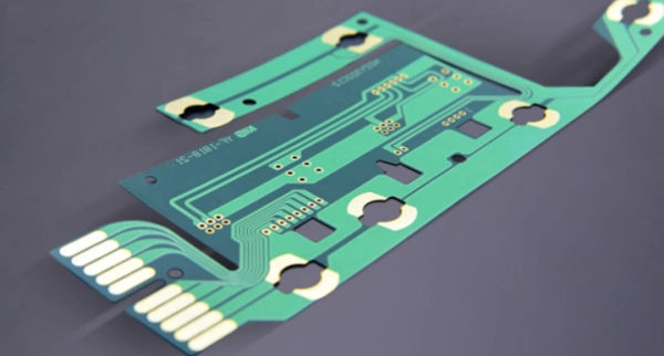
PCB warpage is usually caused by a combination of design, material, and manufacturing factors.
1. Uneven Copper Distribution
Copper layers significantly influence PCB mechanical stability. When copper areas are not balanced between layers, different regions of the PCB experience different levels of stress during heating and cooling.
For example, a multilayer PCB with large copper planes on one side and limited copper on the opposite side may experience uneven shrinkage, increasing the risk of warpage.
2. Material Selection and CTE Mismatch
Different PCB materials expand and contract at different rates during temperature changes. The coefficient of thermal expansion (CTE) mismatch between copper, laminate materials, and components can generate internal stress.
High-performance applications using materials such as high-frequency laminates, low-loss materials, or mixed-material stack-ups require careful material selection and stack-up optimization to reduce deformation risks.
3. Improper PCB Stack-Up Design
A balanced PCB stack-up helps maintain mechanical stability.
Common stack-up issues include:
- Asymmetrical layer arrangement
- Uneven dielectric thickness
- Imbalanced copper weight
- Improper prepreg selection
For multilayer boards, maintaining symmetry between the top and bottom layers is an important factor in controlling warpage.
4. Thermal Stress During Manufacturing
PCB manufacturing involves multiple thermal processes, including:
- Lamination
- Reflow soldering
- Wave soldering
- Thermal cycling
During these processes, repeated heating and cooling can release internal stress within the PCB structure, resulting in deformation.
5. Large Components and Assembly Conditions
During PCBA assembly, heavy components such as connectors, transformers, and power devices can increase mechanical stress on the PCB.
In SMT production, excessive PCB warpage may cause:
- Poor solder paste printing
- Component placement errors
- Insufficient solder joints
- Open circuits or solder defects
How Does PCB Warpage Affect Manufacturing?
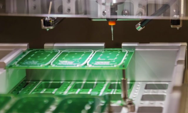
PCB warpage can directly impact production efficiency and product reliability.
SMT Assembly Challenges
Modern SMT equipment requires a relatively flat PCB surface for accurate printing and component placement. Excessive warpage may create gaps between the PCB and production fixtures, affecting solder paste consistency.
Reduced Assembly Yield
Warpage-related defects may include:
- Misaligned components
- Solder bridging
- Open solder joints
- BGA connection failures
For fine-pitch components such as BGAs and CSPs, PCB flatness becomes even more critical.
Mechanical Reliability Risks
A warped PCB may experience additional stress during installation, enclosure integration, and long-term operation, potentially reducing product lifetime.
How to Control PCB Warpage?
Effective warpage control requires cooperation between PCB design, fabrication, and assembly processes.
1. Optimize PCB Stack-Up Design
Engineers should consider:
- Symmetrical layer structures
- Balanced copper distribution
- Appropriate dielectric thickness
- Suitable laminate materials
A well-designed stack-up reduces internal stress and improves dimensional stability.
2. Perform DFM Review Before Manufacturing
Early DFM analysis helps identify potential warpage risks before production.
A professional PCB manufacturer may review:
- Copper balance
- Layer symmetry
- Board thickness
- Material compatibility
- Panel arrangement
This allows design adjustments before expensive manufacturing or assembly stages.
3. Improve Manufacturing Process Control
Manufacturers can reduce PCB warpage through:
- Controlled lamination parameters
- Proper curing cycles
- Optimized panel design
- Improved handling procedures
- Flatness inspection
4. Consider Assembly Requirements
For high-density PCBA products, PCB design should consider:
- SMT equipment requirements
- Component weight distribution
- Reflow temperature profiles
- Fixture support methods
This ensures better production stability and reduces assembly defects.
PCB Warpage Considerations for High-Reliability Applications
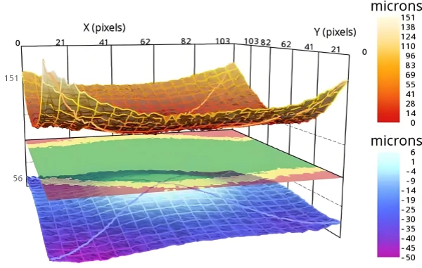
In industries such as automotive electronics, industrial control, communication systems, and semiconductor testing equipment, PCB flatness directly influences product reliability.
Complex boards involving:
- High layer counts
- HDI structures
- High-frequency materials
- Mixed copper weights
- Large mechanical components
require more detailed engineering evaluation to maintain dimensional stability.
Conclusion
PCB warpage is not only a fabrication issue but also a system-level manufacturing consideration. It can influence SMT assembly quality, electrical reliability, and overall production yield.
By optimizing PCB stack-up design, balancing copper distribution, selecting suitable materials, and conducting early DFM reviews, manufacturers can significantly reduce warpage risks and improve production consistency.
At KKPCB, engineering support during PCB design review and manufacturing preparation helps customers identify potential warpage challenges early and achieve more reliable PCB/PCBA production outcomes.
