HomeCategory

PCB Design Services | Professional PCB Layout & Design - KKPCB

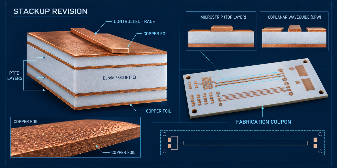
Duroid 5880 PCB Stackup: 6 Critical Controls for Stable Impedance Release

Contents Why stackup drift changes RF behavior Six stackup and impedance controls Coupon and release workflow Release checklist Duroid 5880 PCB stackup decisions determine whether an RF design can move from field model to repeatable fabrication. A nominal dielectric value is not enough. Pressed thickness, copper foil, roughness, trace geometry, and coupon correlation all influence...
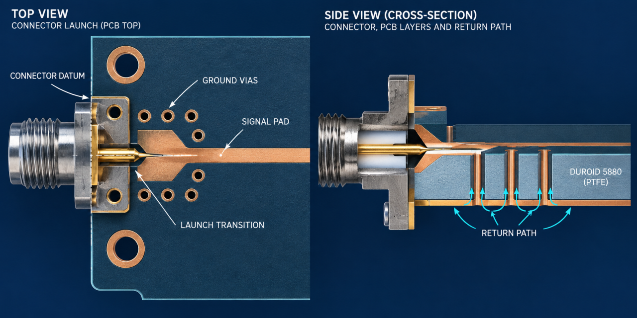
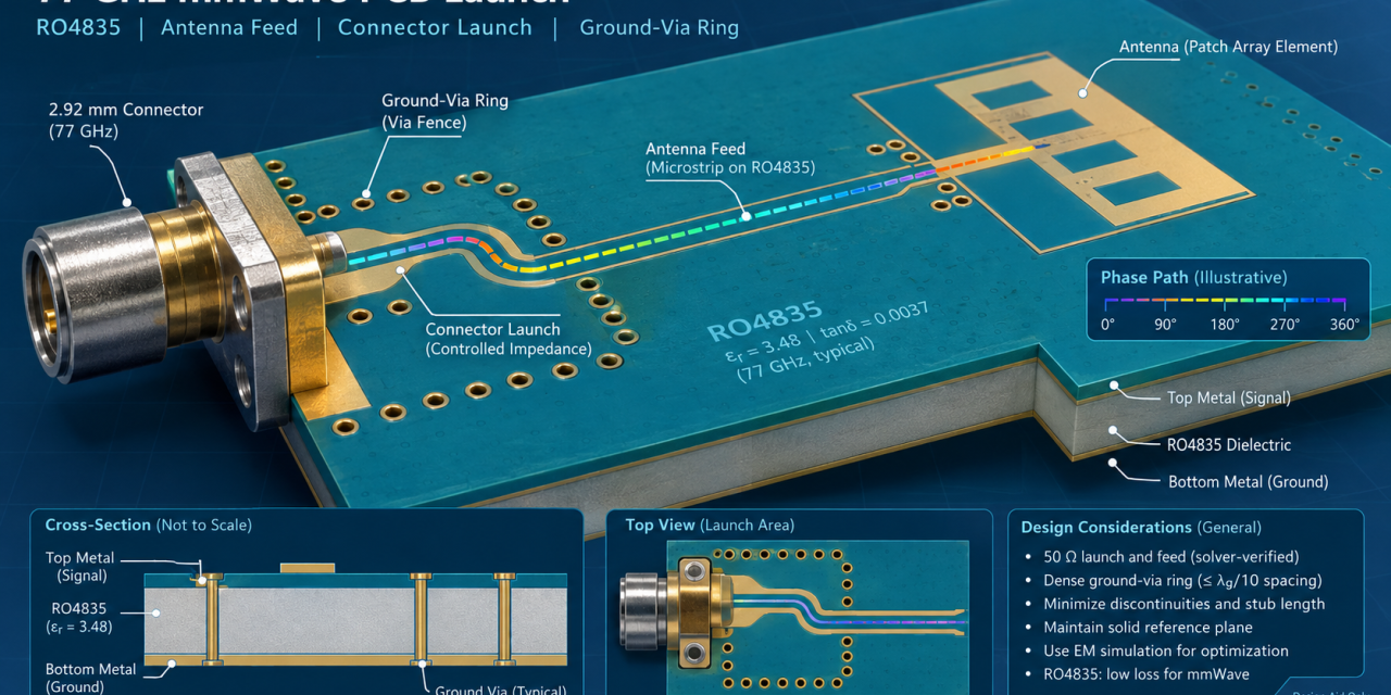
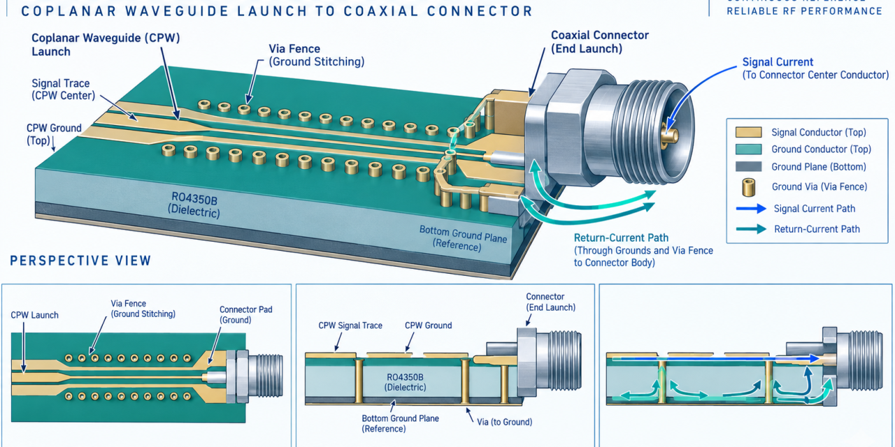
Duroid 5880 PCB Connector Launch: 8 Critical Controls for Repeatable RF Assembly

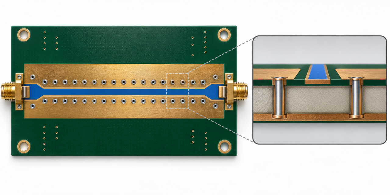
Contents Why the connector launch controls RF yield Layout and datum controls Assembly and inspection controls Release checklist Duroid 5880 PCB connector launches are a common project pain point. A layout can meet the simulated impedance target and still show return-loss variation when the connector datum, plated holes, solder fillet, or ground-via pattern changes during...

Duroid 5880 PCB Dimensional Stability: 7 Critical Controls

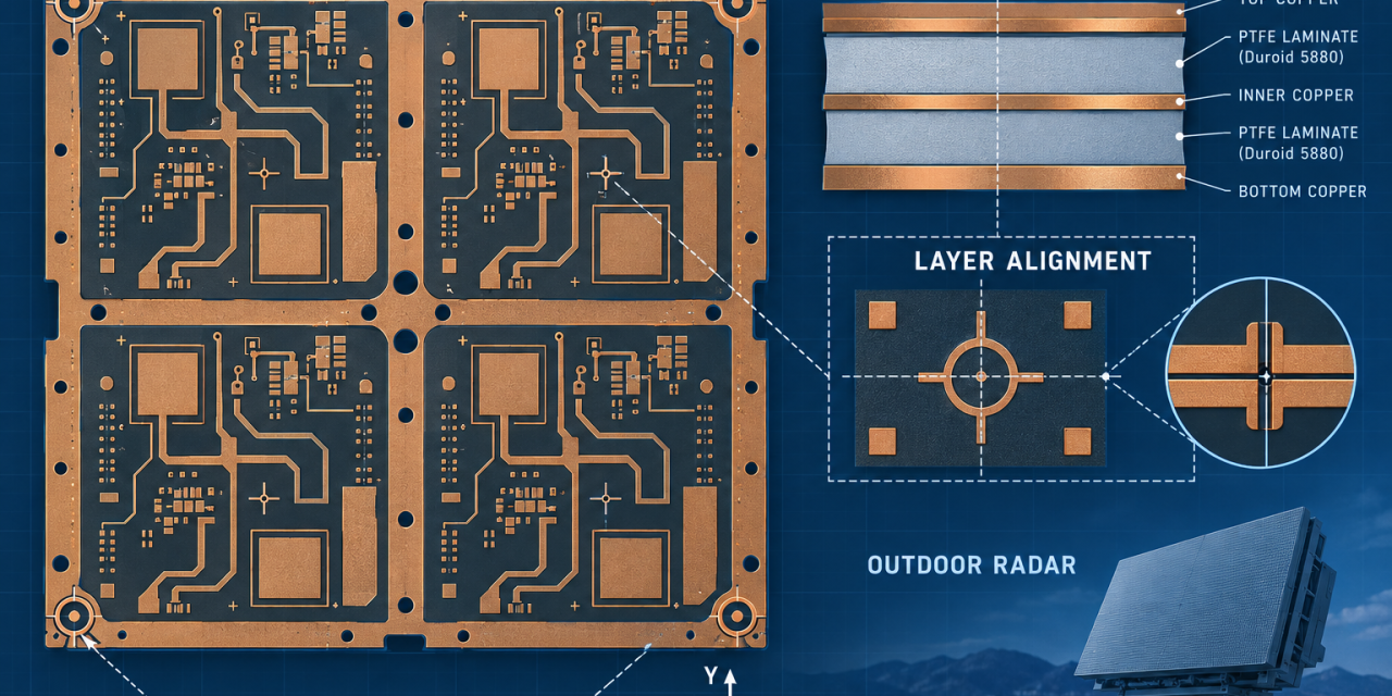
Contents Why dimensional stability becomes an RF problem Seven production controls Outdoor radar release checklist Key takeaway Duroid 5880 PCB projects for outdoor radar often fail at the mechanical-to-RF interface rather than in the laminate specification. Seasonal temperature, moisture conditioning, panel handling, and connector datum changes can move a launch or array cell enough to...

RO5880 PCB Dimensional Stability: Managing Moisture and Registration in Outdoor Radar

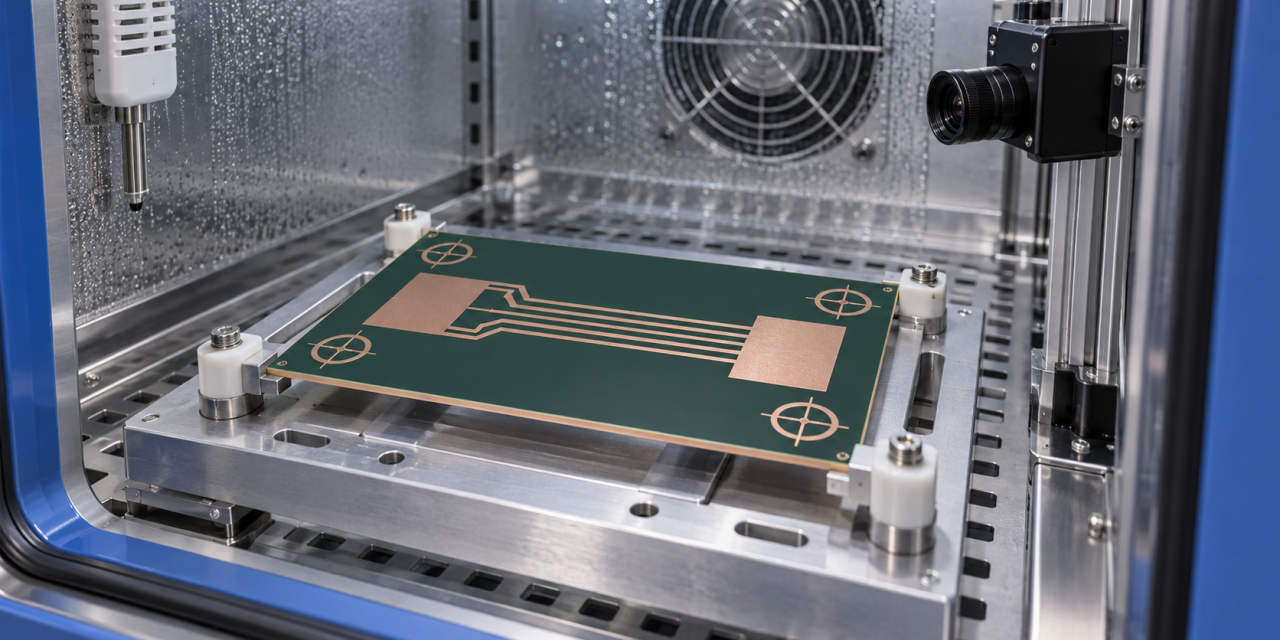
Outdoor radar and microwave equipment can see humidity, temperature swings, and repeated handling before a board reaches final system test. For a PTFE-based laminate, the project risk is not only RF loss; it is whether the finished RO5880 PCB keeps its layer registration, connector datum, and antenna geometry through the approved process. This RO5880 PCB...

RO4835 PCB HDI Microvia Design for Thin Radar Modules

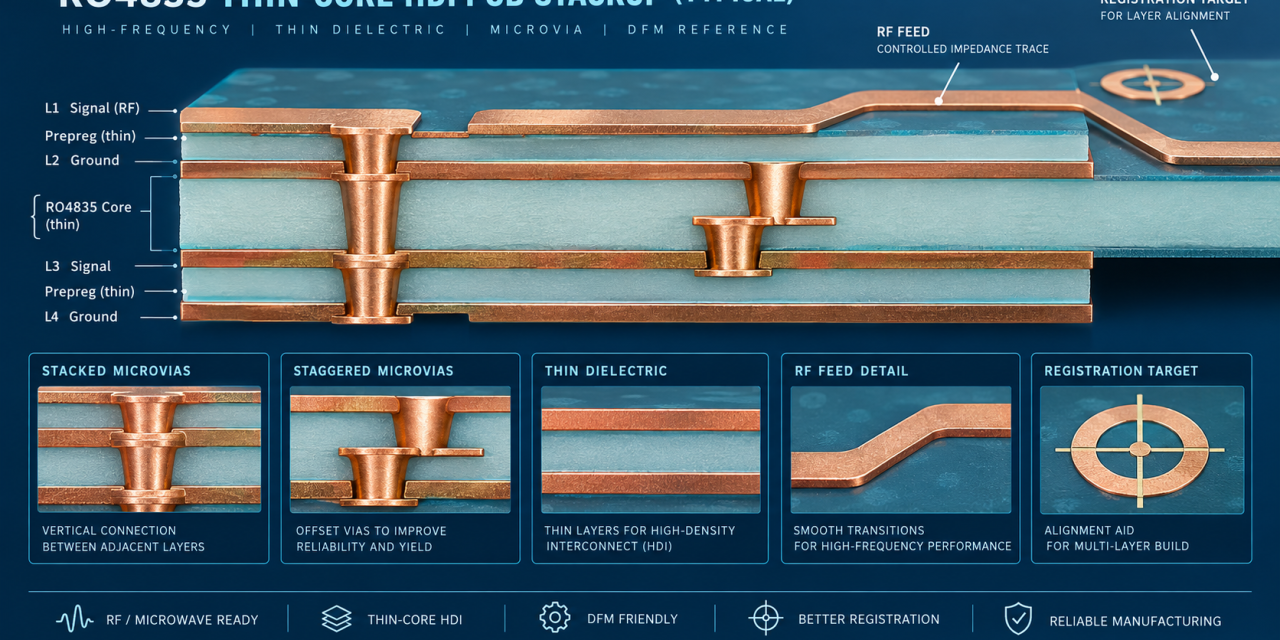
Thin radar modules often force an uncomfortable trade-off: the RF launch wants a stable reference plane while the mechanical envelope pushes the stackup toward finer features. This engineering guide uses the RO4835 PCB to explain how an HDI build can be reviewed without confusing design intent with measured qualification data. Define the thin-module constraint first...

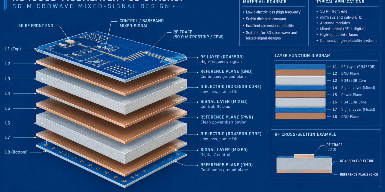
RO4350B PCB Stackup Selection for 5G and Microwave Mixed-Signal Boards

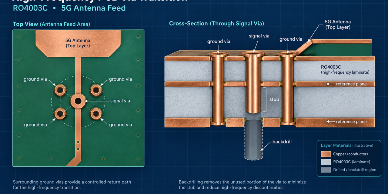
When a radio board combines a 5G front end, clock distribution, and digital processing, stackup selection becomes a system decision rather than a material shortcut. An RO4350B PCB can provide a predictable RF foundation, but only when the chosen dielectric thickness, copper, reference planes, and mixed-signal boundary are carried consistently into fabrication. This guide gives...