
At microwave frequencies, a via fence is part of the RF circuit, not a decorative row of ground holes. A production Duroid 5880 PCB must keep the signal field, return path, connector launch, and fabrication tolerances aligned. This guide addresses the common project pain point of a layout that simulates correctly but loses return-path consistency during drilling, plating, and panel release.
Contents
Define the return path before placing the fence
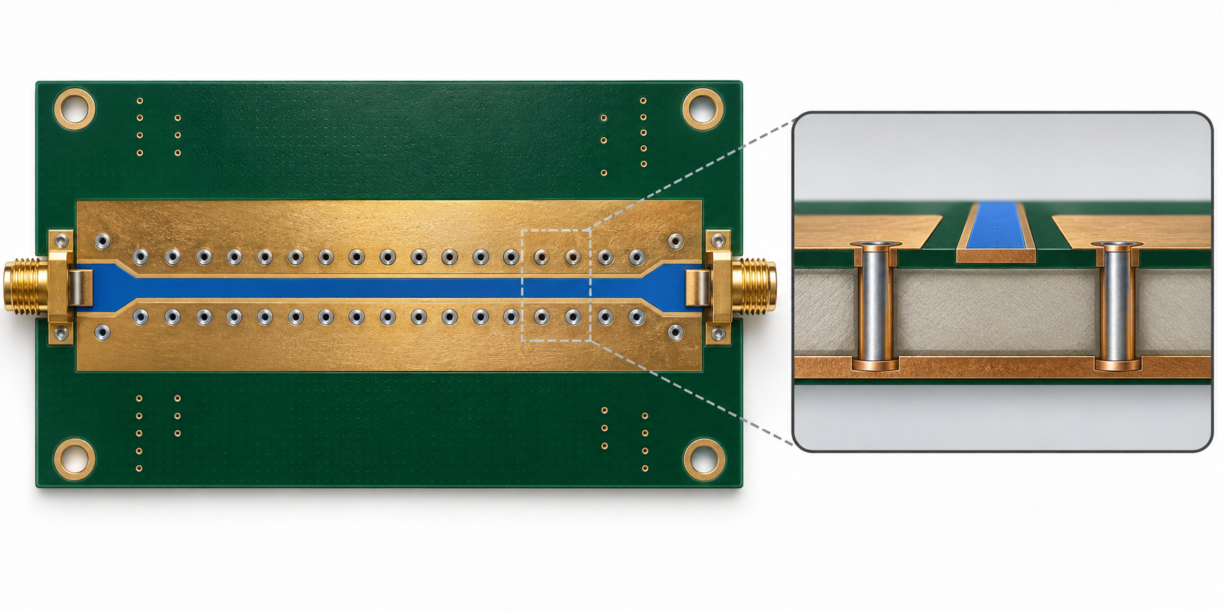
A grounded coplanar waveguide or microstrip transition needs a known reference plane. Start by identifying the plane that carries the return current, then place the fence around the field boundary shown by the RF model. A grounded coplanar waveguide review should show the trace, ground copper, reference plane, and stitching-via connection as one structure.
Rogers lists typical RT/duroid 5880 properties, but material data alone does not define a fence spacing. Treat the model as a design target and verify the finished stackup, copper, and plated-via geometry on the approved Duroid 5880 PCB construction. If the dielectric thickness or copper roughness changes, rerun the field review.
Control spacing and transitions
Use a rule tied to the field, not a copied grid
Keep the fence close enough to contain the return field while preserving the drill, annular-ring, and solder-mask clearances required by fabrication. The spacing should be documented with the trace width, dielectric reference, and via diameter. A high-frequency PCB check should compare fence placement at straight runs, bends, tapers, and transitions.
Manage layer changes deliberately
When a signal changes layers, give the return current a nearby path through the same transition. Avoid a fence break directly over a reference-plane void or connector keep-out. If the board uses back-drilled or sequential structures, show which vias stop at each layer and how the return current crosses the build.
Coordinate the connector launch
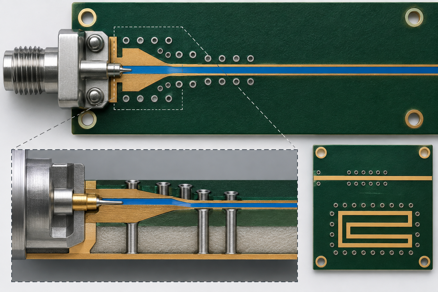
The connector launch is often where an otherwise regular fence becomes irregular. Share one mechanical datum for the connector, signal pad, ground pads, mounting holes, and first fence vias. Keep the launch footprint and RF model synchronized when the connector supplier changes. The RF connector assembly traveler should also identify seating, torque, solder, or inspection requirements that can change the launch geometry.
Use a representative launch coupon when the project requires electrical correlation. Define fixture, calibration, frequency range, and acceptance method before production. A coupon is process evidence, not a fabricated customer measurement.
Make the fence manufacturable
Every via in the fence must fit the drill, plating, and registration process. Each Duroid 5880 PCB panel should carry the same via-fence revision. Review finished hole, aspect ratio, annular ring, copper balance, and the distance to routed edges. For a PCB manufacturing handoff, identify the master datum, tooling holes, fiducials, drill program, lamination revision, and surface finish. Keep the via-fence geometry visible on both individual-board and panel drawings.
Inspect representative center and edge locations when panel density or copper fill changes across the panel. Cross-section coupons can confirm layer order and plated-via continuity. Separate typical material information, engineering targets, and measured evidence in the report so a process witness is not misread as a product qualification.
Duroid 5880 PCB via-fence checklist
- Identify the reference plane and return-current path before placing vias.
- Document trace, dielectric, via, and fence-spacing relationships.
- Provide a nearby return path at every layer transition.
- Share a connector datum across layout, tooling, assembly, and inspection.
- Review drill, plating, annular ring, and registration capability.
- Trace any RF coupon to panel position, material lot, and process revision.
KKPCB can review a multilayer Duroid 5880 PCB via-fence package for stackup, return-path continuity, connector transitions, and panel DFM. The objective is a fence that remains electrically meaningful and manufacturable through volume release for every Duroid 5880 PCB lot.
Key takeaway
A stable via fence is a coordinated RF, mechanical, and fabrication decision. When the field boundary, return plane, connector datum, drill process, and inspection evidence are locked together, a Duroid 5880 PCB can move from modeled prototype to repeatable production with fewer return-loss surprises.
Sources: Rogers Corporation RT/duroid 5880 material information and fabrication guidance; IPC-TM-650 methods for drilling, plating, registration, and cross-section inspection; KKPCB internal high-frequency DFM capability notes. Values are typical or target references unless explicitly identified as measured.
