
Thin radar modules often force an uncomfortable trade-off: the RF launch wants a stable reference plane while the mechanical envelope pushes the stackup toward finer features. This engineering guide uses the RO4835 PCB to explain how an HDI build can be reviewed without confusing design intent with measured qualification data.
Define the thin-module constraint first
An RO4835 PCB HDI design should freeze the finished dielectric, copper distribution, laser-via layers, and component keep-outs before routing. A thin core can improve form factor, but it also changes reference height and may narrow the process window for impedance. The stackup owner must therefore control both electrical and manufacturability assumptions.
| Constraint | Failure mode | Review evidence |
|---|---|---|
| Thin dielectric | Impedance shifts after press | Released construction and coupon plan |
| Microvia capture | Open or weak interconnect | Pad, drill, and fill rule review |
| RF escape | Return-path discontinuity | Layer-by-layer launch inspection |
| Panel utilization | Warp or registration loss | Copper-balance and array review |
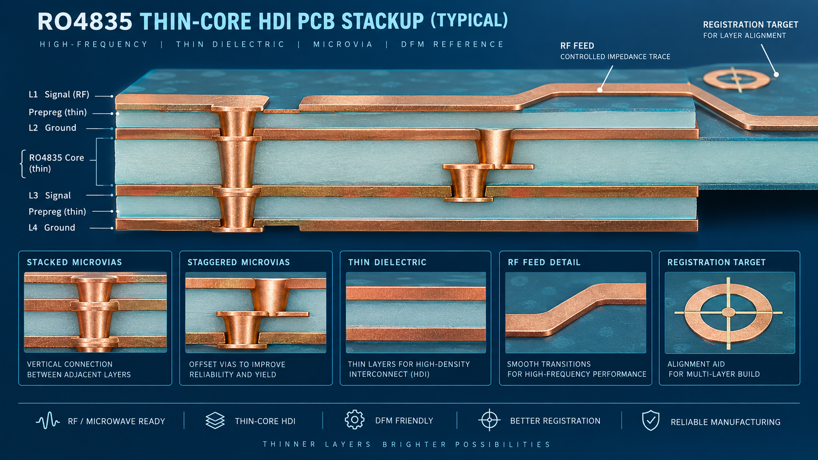
Illustrative thin-module stackup with RF reference planes and laser-microvia transitions.
Use microvias to preserve the RF return path
Microvias are most useful when they shorten a connection without forcing the RF signal across an unnecessary plane change. Keep ground stitching near the signal transition and check capture-pad geometry against the released dielectric. The RO4835 PCB escape must be reviewed as a complete current path, not as a collection of isolated holes.
HDI review sequence
- Assign each laser-via layer and its reference plane in the stackup drawing.
- Check capture-pad, land, and annular-ring rules against the fabricator design rules.
- Confirm filled-via requirements under fine-pitch pads and thermal lands.
- Keep the RF launch and its ground return within the same controlled transition zone.
- Review sequential lamination notes with the actual panel build owner.
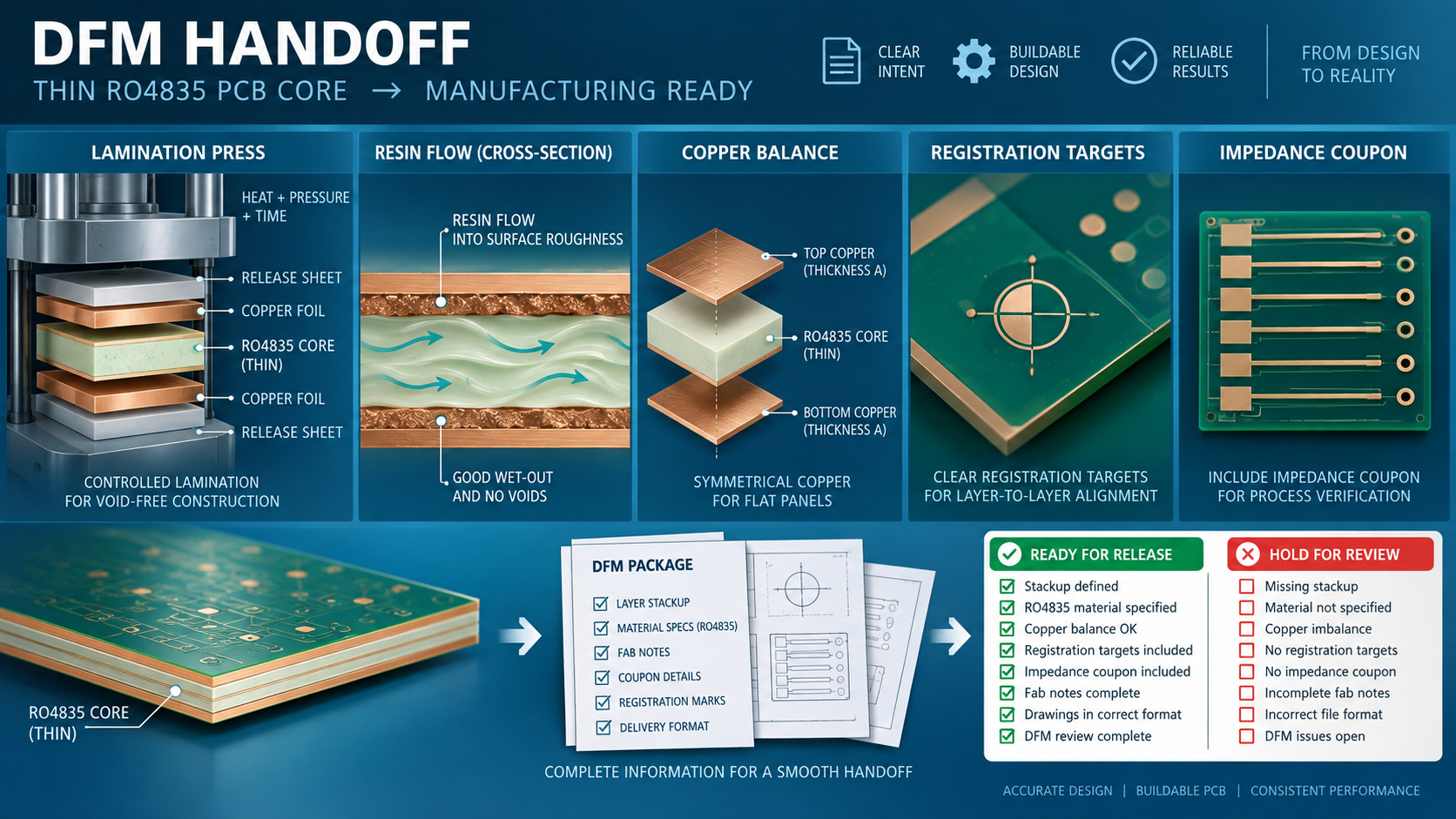
Illustrative thin-core DFM view showing microvia keep-outs, copper balance, and assembly clearance.
Separate coupon evidence from material data
For a controlled impedance PCB, the coupon should represent the critical line width, dielectric height, and copper treatment used by the product. Vendor-typical dielectric data can guide the model, but it is not a project measurement. A release package should identify the coupon method, calibration, sample count, and acceptance tolerance.
DFM checks for thin HDI panels
The multilayer PCB review should cover registration between sequential lamination cycles, copper balance, drill wander, solder-mask clearance, and edge routing. If the product includes an RF shield or stiffener, add those mechanical datums before approving the array.
- Compare the laser-via map with the latest component land pattern.
- Check copper thieving and balance around dense radar channels.
- Confirm solder-mask definition where pad-to-pad spacing is limited.
- Record backdrill or stub controls for any through-via crossing the RF path.
- Assign an ECO owner for every layer-count or via-type change.
Example design-to-production handoff
In an illustrative project, engineering can freeze the RO4835 PCB layer map, impedance intent, and microvia reliability assumptions before purchasing requests a quotation. The PCB manufacturing traveler should then carry the same revision, with deviations linked to a named approver. These are planning controls, not claimed customer results.
Questions project teams ask
Does a thinner core always improve RF performance?
No. It changes field distribution, loss, and impedance sensitivity; the full stackup and return path must be rechecked.
Can every microvia be filled?
Only when the released process, pad geometry, and reliability requirements support it. Confirm the rule with the fabricator.
What is the best acceptance evidence?
Use representative coupons, dimensional inspection, and a traceable report that distinguishes targets from measured values.
Sources: Vendor-typical RO4835 material context and KKPCB public High-Frequency PCB, HDI PCB, PCB Materials, Multilayer PCB, and PCB Manufacturing categories. No external hyperlinks or claimed customer measurements are used.
For the final RO4835 PCB handoff, keep the RO4835 PCB microvia map, stackup, coupon definition, and inspection plan in one controlled release.
Keep the RO4835 PCB HDI stackup, RO4835 PCB microvia map, RO4835 PCB RF escape, RO4835 PCB coupon, and RO4835 PCB inspection record on one revision.
