
At 77 GHz, a promising RF launch can lose margin when the transition, return path, and enclosure reference are treated as separate tasks. This guide uses the RO4835 PCB as an engineering example for a radar launch that can be reviewed before fabrication. The geometry is illustrative, not a customer measurement.
Start with the launch interface, not the laminate label
The RO4835 PCB should be released with finished dielectric assumptions, copper treatment, line width after etch compensation, and the connector or antenna reference plane. A launch fails when the field-solver model uses one reference height while the drawing gives the fabricator another. Freeze the stackup revision before tuning the taper.
| Launch item | Typical risk | Design-control action |
|---|---|---|
| Reference plane | Return current detours | Keep a continuous ground path under the transition |
| Neck-down | Local impedance step | Control width, clearance, and pad escape together |
| Via fence | Parallel-plate leakage | Place stitching vias around the launch envelope |
| Connector land | Unmodeled capacitance | Use the released footprint in the EM review |
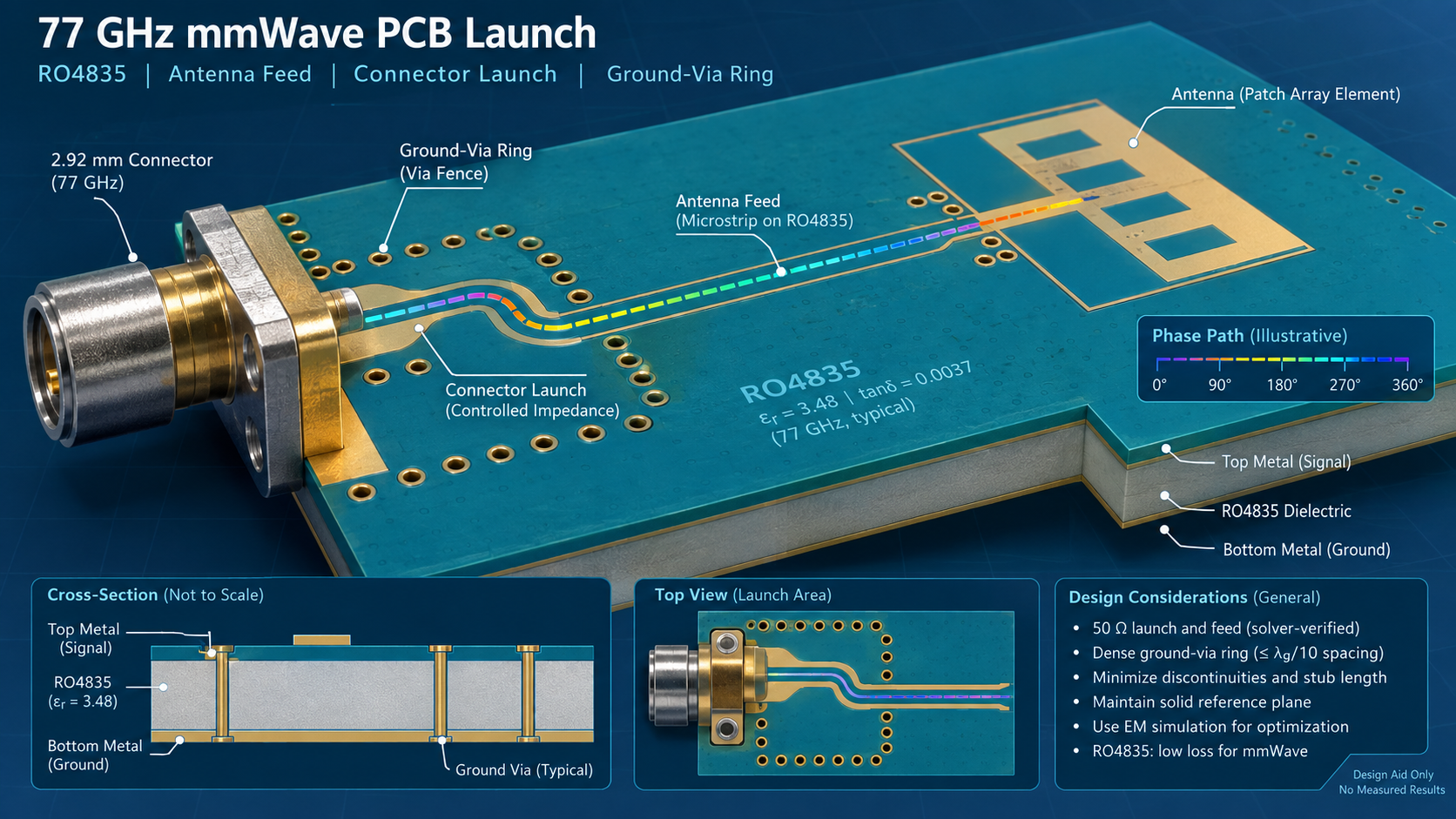
Illustrative 77 GHz launch transition showing the signal taper, reference plane, and via-fence boundary.
Control return current through the transition
A 77 GHz launch is a current-path problem as much as a trace-width problem. Keep ground vias close enough to provide a low-inductance path, but verify drill, pad, and anti-pad clearances against the released stackup. The controlled impedance PCB review should include the connector pin field and the first bend, not only the straight microstrip.
Via-fence review questions
- Does every signal-layer transition have a nearby ground-via return?
- Are via barrels and anti-pads clear of the launch field?
- Does the fence remain manufacturable after solder-mask and edge-clearance rules are applied?
- Is the enclosure contact defined as a mechanical datum rather than an assumed ideal ground?
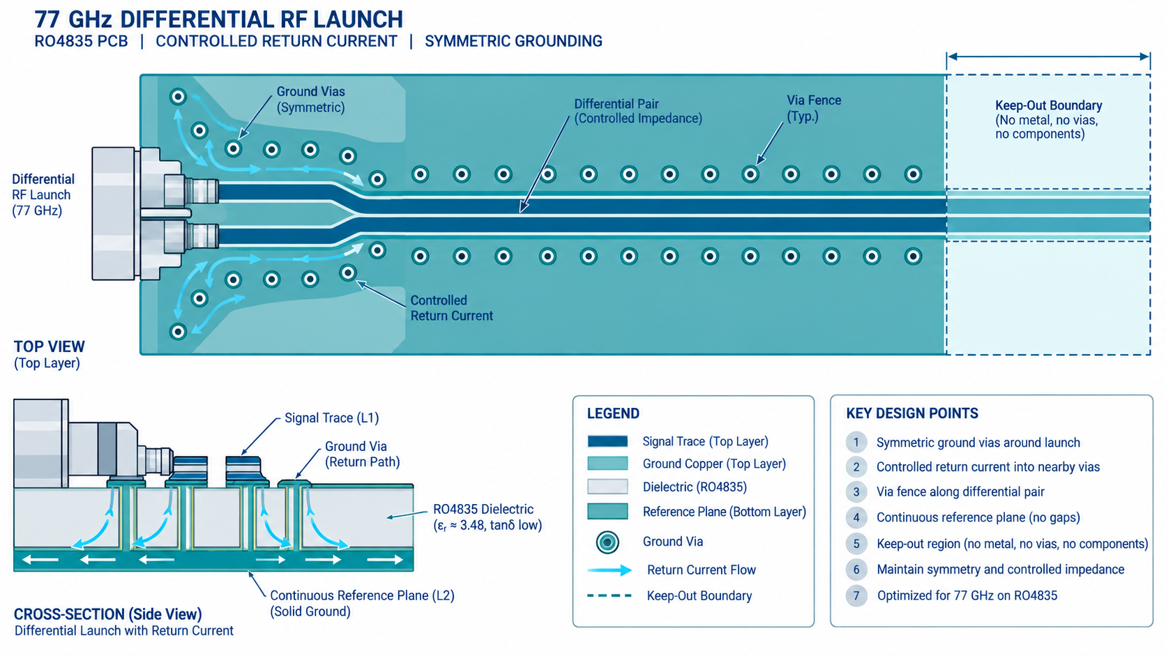
Illustrative via-fence and return-current concept for an RF connector transition.
Use simulation targets without inventing test results
For an RF launch release, separate modeled targets from measured evidence. A field-solver or 3D model can define expected reflection and phase behavior; a production report must identify calibration, fixture, sample size, and environmental conditions. Do not label a design target as an achieved insertion-loss result.
DFM checks before the launch is frozen
The multilayer PCB review should confirm registration, finished copper, drill-to-copper clearance, and local copper balance. For a HDI PCB escape, add microvia capture-pad and fill rules to the same launch checklist.
- Verify the connector footprint against the released mechanical model.
- Check the taper after etch compensation and solder-mask definition.
- Keep the ground reference uninterrupted below the critical transition.
- Document controlled-depth or backdrill notes where stubs can resonate.
- Assign an ECO owner for any launch geometry change.
Example acceptance gates for a radar project
In an example project plan, the engineer can require stackup sign-off, launch coupon review, drawing-to-CAD comparison, and first-article inspection before volume release. The RO4835 PCB package should identify which values are design targets, which are vendor-typical material data, and which are project measurements. This keeps procurement decisions traceable without claiming a customer case.
Questions from RF and mechanical teams
Should the via fence be tuned only by spacing?
No. Via diameter, antipad, layer transition, enclosure ground, and local dielectric height all influence the return path.
Can a connector footprint be copied between stackups?
Only after the reference height, pad geometry, and launch model are rechecked for the new construction.
What must be frozen before fabrication?
Freeze the stackup, launch footprint, critical dimensions, impedance intent, and deviation authority in one revision.
Sources: Vendor-typical RO4835 material context and KKPCB public High-Frequency PCB, PCB Materials, PCB Manufacturing, Multilayer PCB, HDI PCB, and RF design categories. No external hyperlinks or claimed customer measurements are used.
For the final RO4835 PCB release, keep the RO4835 PCB launch drawing, stackup, return-path notes, and inspection plan on the same controlled revision.
Keep the RO4835 PCB launch model, RO4835 PCB stackup, RO4835 PCB via fence, RO4835 PCB connector footprint, and RO4835 PCB acceptance note on one revision.
