
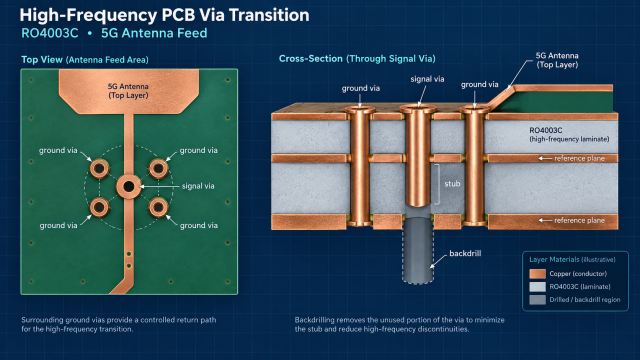
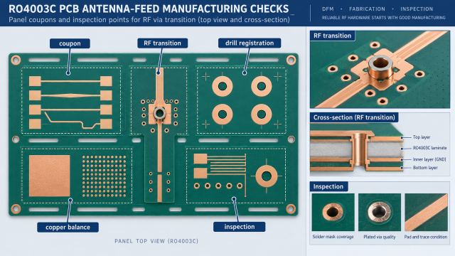
 A 5G antenna feed can pass a nominal impedance check and still lose margin when a plated via, unused barrel, or poor ground return is introduced at the layer transition. This guide uses the RO4003C PCB as an engineering example for controlling via stubs, return current, and production handoff. The figures are illustrative design aids, not customer measurements.
Why a via transition changes the RF budget
The RO4003C PCB stackup should define the signal layer, reference planes, finished dielectric, copper treatment, and any backdrill depth before the antenna feed is routed. A through-via that crosses unused layers adds a stub and can create a resonance in the operating band. The transition therefore belongs in the stackup review, not only in the layout cleanup phase.
| Transition item | Typical risk | Design-control action |
|---|---|---|
| Via stub | Resonant discontinuity | Limit stub or specify controlled backdrill |
| Reference plane | Return-current detour | Place ground vias beside the signal via |
| Antipad | Excess capacitance | Review clearance against the released stackup |
| Launch pad | Impedance step | Tune pad, neck-down, and mask together |
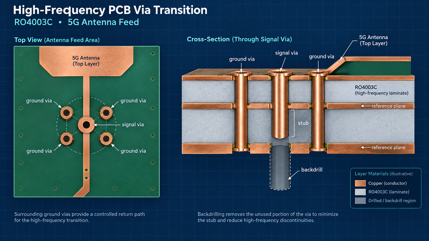
Illustrative RO4003C PCB via transition for a 5G antenna feed, showing signal, ground, reference planes, stub, and backdrill intent.
Keep the return path close to the signal via
At a layer change, the multilayer PCB return current must move between reference planes without a long detour. Place one or more ground vias close to the signal via, then check drill-to-copper and anti-pad clearances against fabrication rules. A nominal via-fence pitch is not a substitute for reviewing the actual current path and enclosure interface.
RF transition review sequence
- Mark the signal via, ground vias, and reference-plane changes in the stackup drawing.
- Estimate the remaining stub after the planned backdrill or sequential build.
- Check the antenna-feed pad and neck-down after etch compensation.
- Verify the via field remains clear of mechanical fasteners and shielding features.
- Assign an ECO owner for every transition geometry change.
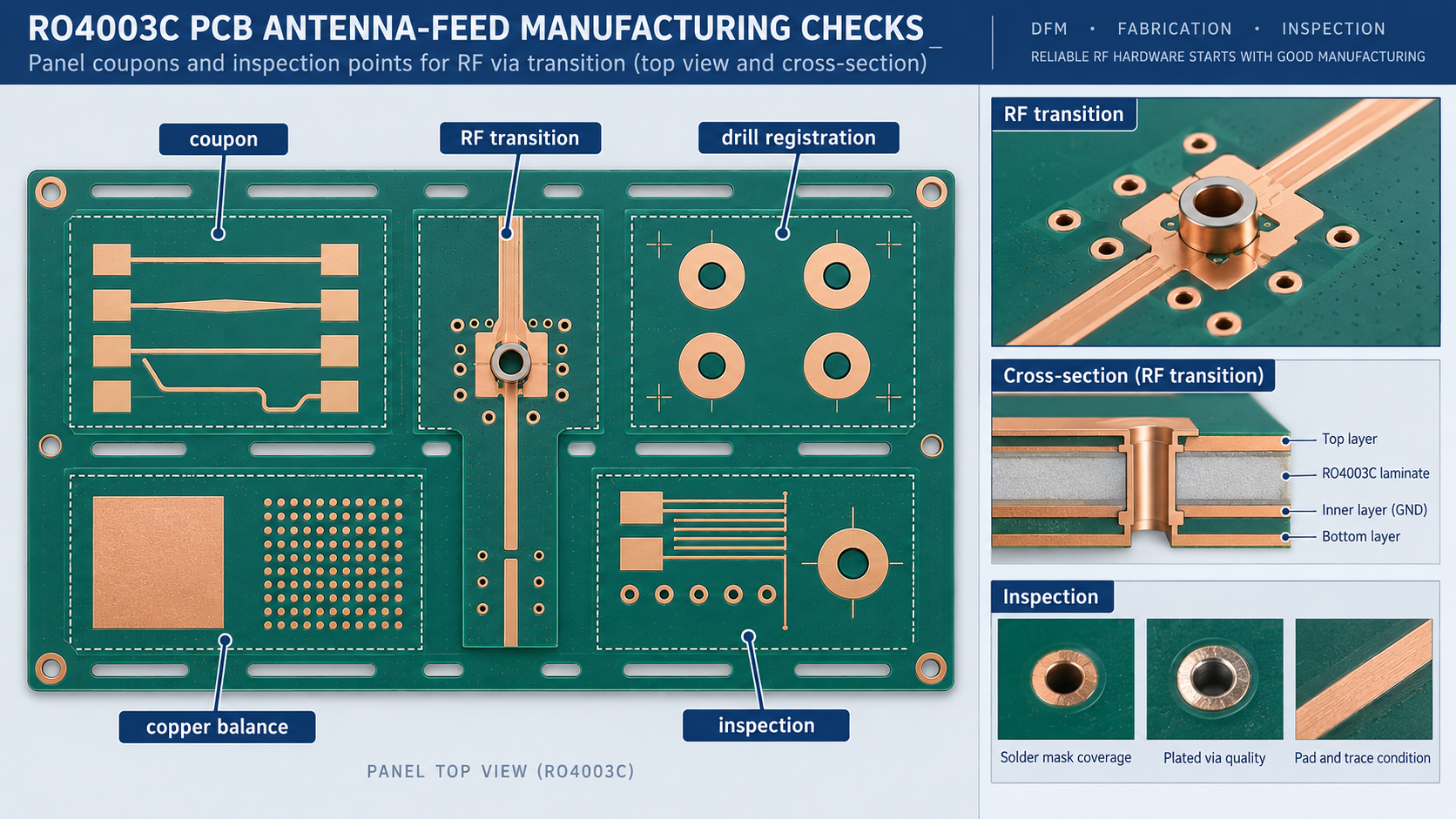
Illustrative DFM and coupon inspection view for an RF via transition panel.
Use a representative coupon, not a generic promise
For a controlled impedance PCB, the coupon should reproduce the critical line width, reference height, copper class, and plating exposure of the antenna feed. Separate a field-solver target from a measured coupon result. A project report should state fixture, calibration, sample size, and environmental conditions before any value is called measured.
DFM checks before releasing the antenna feed
The HDI PCB option can shorten the transition, but laser-via capture pads, sequential lamination, and fill requirements must be explicit. The PCB materials review should also check finished thickness and copper balance around the RF region.
- Compare the released drill file with the via-transition map.
- Check annular ring, registration, and backdrill-depth tolerances.
- Keep copper balanced to limit panel bow and twist.
- Document mask openings and edge clearances around the antenna feed.
- Link deviations to the correct drawing revision before purchasing release.
Example project handoff
In an illustrative 5G module program, the RO4003C PCB package can require stackup sign-off, transition review, coupon definition, drawing-to-CAD comparison, and first-article inspection. These gates help an engineering team distinguish design targets, vendor-typical material data, and project measurements without claiming a customer case.
Questions from RF and manufacturing teams
Is backdrilling always required?
No. It depends on the remaining stub, operating band, layer transition, and the tolerance that the released design can accept.
Can the ground via be placed anywhere near the signal via?
No. Its location, anti-pad, and connection to the receiving reference plane determine whether it provides a useful return path.
What must be frozen before fabrication?
Freeze the stackup, via map, backdrill note, coupon geometry, inspection method, and deviation authority in one revision.
Sources: Vendor-typical RO4003C material context and KKPCB public High-Frequency PCB, PCB Materials, Multilayer PCB, HDI PCB, and PCB Manufacturing categories. No external hyperlinks or claimed customer measurements are used.
For the final RO4003C PCB release, keep the RO4003C PCB via-transition drawing, coupon definition, backdrill note, and inspection record under one controlled revision.
