
When a radio board combines a 5G front end, clock distribution, and digital processing, stackup selection becomes a system decision rather than a material shortcut. An RO4350B PCB can provide a predictable RF foundation, but only when the chosen dielectric thickness, copper, reference planes, and mixed-signal boundary are carried consistently into fabrication. This guide gives engineers and project managers a practical way to freeze that decision without presenting unverified KKPCB measurements.
Start with the electrical partition
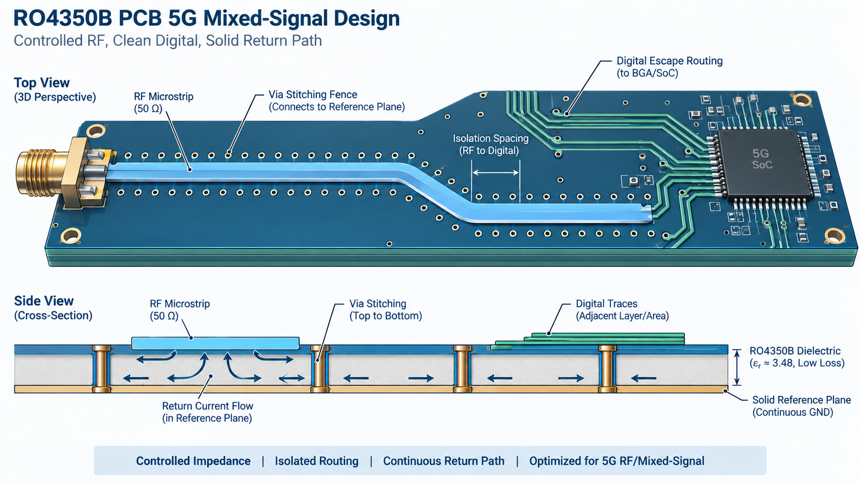
Define the RF path before selecting layer names. Mark antenna feeds, power-amplifier outputs, local oscillators, clock lines, high-speed digital buses, and sensitive receive nodes. A controlled 5G PCB region should have a continuous reference plane and a short return-current path. Digital escape routing can share the board, but it should not force the RF trace across plane splits or an uncontrolled material boundary.
| Stackup decision | Project risk | Release action |
|---|---|---|
| RF dielectric thickness | Nominal thickness is used instead of finished pressed thickness. | Release the finished dielectric target and tolerance to the fabricator. |
| Reference plane | Return current detours around a split, void, or connector keep-out. | Show the RF plane, voids, and transition geometry on the layer review. |
| Copper profile | Etch compensation changes width and effective impedance. | Identify copper weight, treatment, and finished trace assumptions. |
| Digital/RF boundary | Resin flow or via fields change the local electromagnetic environment. | Model the boundary and add it to the DFM checklist. |
Choose finished dimensions, not nominal laminate
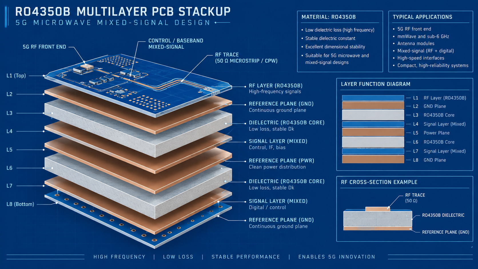
A robust RO4350B PCB stackup starts with finished dielectric height between the RF conductor and its reference plane. Rogers vendor data commonly lists RO4350B process Dk around 3.48 with a design Dk around 3.66 and Df around 0.0037; these are vendor-typical values, not a KKPCB lot measurement. The field-solver model must state which value, frequency, copper profile, and finished thickness were used.
Do not let a 5G PCB drawing say only “RO4350B core.” Identify the laminate family, pressed thickness, copper foil, surface finish, and solder-mask treatment that affect the released geometry. If a material substitution is proposed, update the impedance and loss model before approving the change.
Keep the return plane continuous
For each RF trace, identify the nearest solid reference plane and the exact path taken by return current through launches, vias, and component pads. A controlled impedance PCB rule is useful only when the plane geometry is controlled as well. Avoid routing a feed over a split simply because the width meets a calculator result; the discontinuity can dominate the transition.
Plan the mixed-signal boundary
Many 5G modules place RF layers in RO4350B and digital layers in standard cores. This hybrid approach can be practical, but the boundary must be explicit. A multilayer PCB release should show where resin distribution, plane spacing, and via transitions may change the effective line environment. The released RO4350B PCB stackup should identify which layers are phase- or impedance-critical and which layers are allowed to carry general digital routing.
If the board uses an HDI PCB escape, define whether microvias are stacked or staggered and how capture pads reference the RF plane. Keep bias lines and high-speed clocks away from the antenna feed, and reserve a transition review for every connector, via field, and layer change.
Use DFM to protect the stackup
During the DFM review, compare the stackup file, fabrication drawing, impedance table, and drill data line by line. A fabricator should know the finished dielectric target, copper balance, registration class, surface finish, solder-mask opening, and coupon definition. KKPCB public manufacturing information covers high-frequency and mixed-material PCB services, while the exact process window remains quotation-specific.
When a PCB manufacturing partner proposes a press-cycle or copper change, record it as a controlled engineering change. Do not silently replace a RO4350B PCB core with an equivalent material and keep the old trace width; the electromagnetic model and acceptance criteria belong to the exact released build.
Illustrative project decision: a 5G radio board
Imagine a 5G radio card whose first prototype meets the simulated insertion-loss target, but the production panel shows a wider phase spread between antenna channels. This is an illustrative failure mode, not a KKPCB customer case. The investigation should compare the released stackup, pressed cross-section, copper profile, connector transition, and impedance coupon. If the RF core thickness or resin distribution changed, the team should update the field-solver model before blaming the component.
A project manager can use the RO4350B PCB handoff as a gate: no release until the material variant, finished dimensions, layer references, coupon, and change owner are named. The same decision record should follow the board from prototype to volume tooling.
Validation sequence
- Freeze the exact RO4350B material variant and frequency-appropriate design Dk source.
- Re-solve impedance and loss with finished dielectric and copper assumptions.
- Review RF transitions, plane continuity, via fields, and mixed-material boundaries.
- Inspect the first-article cross-section and registration against the drawing.
- Measure an approved coupon only when the project quality record contains the result.
Release checklist for project managers
- The released RO4350B PCB drawing names the exact material and finished dielectric.
- RF, digital, and power partitions share a documented reference-plane strategy.
- Impedance tables include copper profile, etch assumption, and test coupon definition.
- Any PCB materials substitution triggers model and DFM review.
- Prototype and production builds use the same acceptance logic.
Questions to resolve before release
Can the digital layers use standard cores?
Yes, if the hybrid boundary, plane spacing, resin distribution, and transition geometry are modeled and included in DFM review.
Is the design Dk a measurement from this board?
No. Vendor-typical or design values must be labeled as such. A measured value may be claimed only when recorded by the project quality system.
What should change when the stackup changes?
Update the RO4350B PCB field-solver model, impedance table, drawings, coupon plan, and acceptance owner before fabrication.
Sources: Rogers RO4350B manufacturer data are used for vendor-typical Dk/Df context; KKPCB public PCB Materials, High-Frequency PCB, HDI PCB, Multilayer PCB, and PCB Manufacturing pages verify service categories. This article contains no external hyperlinks and no claimed KKPCB customer measurement.
Engineering release gate
For a production RO4350B PCB, the design owner should record the material variant, finished dielectric, copper profile, and impedance target in the same release package. This RO4350B PCB decision log helps procurement, fabrication, and test teams review a change without losing the RF intent. Keeping the RO4350B PCB naming consistent across drawings and purchase notes also prevents an unapproved substitute.
RO4350B PCB design sign-off
Before procurement releases the build, the RO4350B PCB stackup, transition notes, and coupon reference should carry the same revision code.
