
HomeTag

Ultrasound PCB - KKPCB

How to Keep a High-Voltage Pulser from Polluting an Ultrasound PCB Receive Path

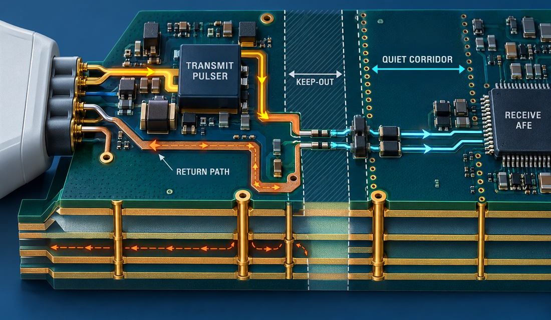
Ultrasound PCB partitioning becomes difficult when the transmit pulser and the receive AFE share a small probe-side area. During a transmit event, a short high-voltage pulse can create a large local current loop, while the receive channel is trying to preserve a much smaller echo signal. If the board treats those two functions as ordinary...
When Ultrasound Echoes Become Layout Noise: A Low-Noise Ultrasound PCB Release Plan

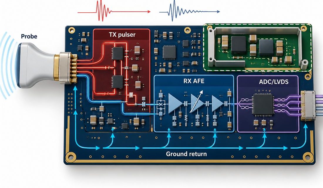
Ultrasound PCB design fails in a very specific way: the image can look acceptable on a bench and then lose contrast when transmit voltage, receive gain, clock activity, and patient-interface cabling are present at the same time. The difficult part is not choosing an expensive AFE; it is preserving the receive signal while the board...