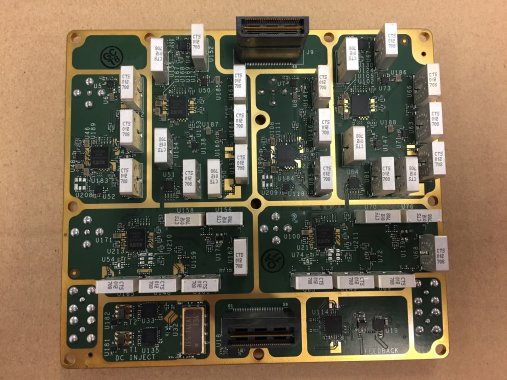
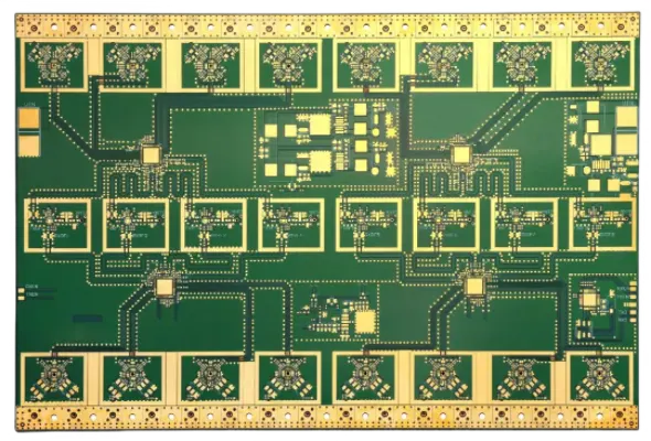
RF PCB design - KKPCB
 
HomeTag

RF PCB design - KKPCB

Thermal Management and Dimensional Stability of RO4003C PCBs in High-Power RF Designs

1. The Growing Thermal Challenge in High-Power RF & mmWave Systems   As 5G infrastructure, satellite communication, and automotive radar systems push beyond 24–81 GHz, PCB substrates face new levels of thermal density and mechanical stress.  In these high-frequency environments, heat is not just a byproduct — it’s a design-defining variable that directly influences signal...

How RO3003 PCBs Are Used in Automotive Radar and 5G Antenna Systems

With the rapid advancement of automotive radar systems and 5G antenna technology, the demand for high-performance RF PCB materials has significantly increased. Among these materials, RO3003 PCB laminates have become a preferred choice for engineers designing high-frequency PCBs due to their low dielectric loss, stable dielectric constant, and excellent thermal reliability. In automotive radar PCB...

Multilayer PCB Manufacturing Process, Advantages and Applications

1. Introduction: Why Multilayer PCBs Are Essential in Modern Electronics As electronic devices continue to evolve toward miniaturization, high-speed performance, and multifunction integration, traditional single-layer or double-layer PCBs can no longer meet design requirements. This has led to the widespread adoption of multilayer PCBs (Multilayer Printed Circuit Boards), which integrate multiple conductive layers within a...

Advanced PCB Footprint Generator: Key to Efficient PCB Design

1. Introduction: Why PCB Footprint Accuracy Matters in Modern Electronics In modern PCB design and electronic product development, accuracy at the earliest design stage directly determines manufacturing success, cost efficiency, and product reliability. One of the most critical elements in PCB layout design is the PCB footprint, which defines the physical land pattern for electronic...