
As smartphones continue to integrate more wireless communication technologies into increasingly compact designs, RF (Radio Frequency) PCB layout and routing have become critical factors affecting overall device performance. Modern mobile phones typically incorporate multiple RF subsystems, including 5G, 4G LTE, Wi-Fi, Bluetooth, GNSS (GPS), NFC, and Ultra-Wideband (UWB), all operating within a limited PCB area.
Unlike conventional digital PCB design, RF PCB layout requires careful consideration of signal integrity, impedance control, electromagnetic interference (EMI), isolation, grounding, and antenna performance. Even minor layout issues can lead to increased insertion loss, degraded receiver sensitivity, reduced transmission power, and certification failures.
This article summarizes practical PCB layout and routing considerations for mobile phone RF designs, focusing on improving signal quality, reducing interference, and supporting reliable high-frequency performance.
1. Characteristics of Mobile Phone RF PCB Design
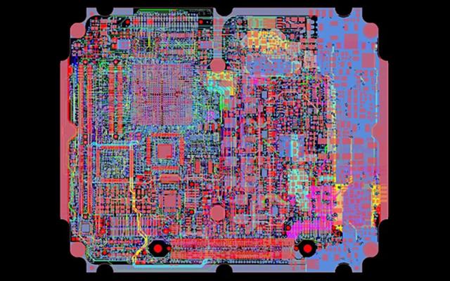
Mobile phone RF boards differ significantly from traditional digital PCBs due to several design constraints:
- Extremely limited PCB space
- Multiple high-frequency RF modules operating simultaneously
- High component density
- Strict impedance control requirements
- Multi-layer HDI PCB structures
- Sensitive coexistence between RF, digital, and power circuits
Because several wireless standards often share the same PCB, minimizing mutual interference is one of the primary design objectives.
2. PCB Stack-Up Planning
A well-designed PCB stack-up provides the foundation for stable RF performance.
Typical considerations include:
- Continuous ground reference planes beneath RF routing
- Controlled dielectric thickness for impedance control
- Separation of RF, digital, and power routing layers
- Minimized discontinuities in return current paths
Modern smartphone PCBs commonly use HDI multilayer stack-ups to accommodate complex routing while maintaining electrical performance.
3. RF Component Placement
Proper component placement is often more important than routing optimization.
General recommendations include:
- Position RF front-end components close to the antenna path.
- Minimize the distance between the RF transceiver and matching network.
- Keep filters, switches, and low-noise amplifiers (LNAs) near their associated RF devices.
- Avoid placing noisy digital circuits adjacent to sensitive RF sections.
A compact and logical RF signal path reduces insertion loss and minimizes unwanted coupling.
4. Controlled Impedance Routing
RF transmission lines should maintain consistent characteristic impedance throughout the signal path.
Common impedance targets include:
- 50 Ω single-ended transmission lines
- 100 Ω differential pairs for applicable high-speed interfaces
Maintaining controlled impedance requires attention to:
- Trace width
- Dielectric thickness
- Copper thickness
- Reference plane continuity
Sudden changes in trace geometry or reference planes may introduce impedance discontinuities and signal reflections.
5. Keep RF Signal Paths Short
High-frequency signals experience increasing loss as routing length increases.
To reduce attenuation:
- Keep RF traces as short as possible.
- Avoid unnecessary routing detours.
- Reduce the number of vias.
- Place matching networks close to RF devices.
Shorter signal paths generally improve transmission efficiency and reduce insertion loss.
6. Via Design Considerations
Each via introduces:
- Additional inductance
- Capacitance
- Impedance discontinuity
Best practices include:
- Minimize the number of RF vias.
- Use optimized via dimensions.
- Add ground stitching vias near RF transitions where appropriate.
- Maintain symmetrical transitions when changing layers.
For millimeter-wave or very high-frequency applications, via optimization becomes increasingly important.
7. Ground Plane Design
Grounding has a significant impact on RF performance.
Recommended practices include:
- Continuous solid ground planes beneath RF traces
- Multiple ground stitching vias surrounding RF sections
- Low-impedance ground return paths
- Elimination of isolated ground islands
Ground discontinuities can increase radiation and degrade signal integrity.
8. Isolation Between RF and Digital Circuits
Digital circuits generate switching noise that may couple into RF signal paths.
To improve isolation:
- Physically separate RF and high-speed digital sections.
- Avoid parallel routing between RF traces and digital buses.
- Isolate switching power supplies from RF circuits.
- Maintain sufficient spacing between noisy and sensitive signals.
Good floorplanning reduces both conducted and radiated interference.
9. RF Power Supply Design
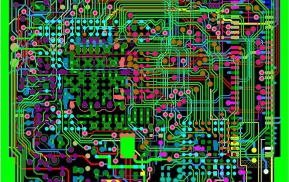
The quality of the RF power supply directly affects receiver sensitivity and transmitter performance.
Power design recommendations include:
- Use low-noise voltage regulators where appropriate.
- Place decoupling capacitors close to RF IC power pins.
- Separate RF power from high-current switching circuits whenever practical.
- Minimize power supply loop area.
Proper filtering helps suppress unwanted noise entering RF circuits.
10. Antenna Layout Considerations
The antenna is one of the most critical components of a smartphone RF system.
PCB recommendations include:
- Maintain the specified antenna clearance area.
- Avoid routing signals beneath the antenna unless specifically permitted by the design.
- Keep metal structures away from the antenna region.
- Preserve the integrity of the antenna matching network.
Mechanical design and PCB layout should be coordinated to achieve optimal radiation efficiency.
11. RF Shielding
Most smartphone RF designs use metal shielding to reduce electromagnetic interference.
Shielding considerations include:
- Place shielding cans over sensitive RF modules.
- Ensure reliable grounding of the shield.
- Avoid creating unwanted resonant cavities.
- Leave sufficient clearance for assembly and inspection.
Shielding helps reduce interference between RF circuits and nearby digital electronics.
12. Thermal Management
High-performance RF components such as:
- Power amplifiers (PAs)
- RF transceivers
- 5G front-end modules
generate significant heat during operation.
Thermal management techniques include:
- Thermal vias beneath power devices
- Large copper heat-spreading areas
- Optimized component placement
- Heat transfer to chassis structures where applicable
Effective thermal design supports both RF performance and long-term reliability.
13. EMI and EMC Considerations
Mobile devices must comply with strict electromagnetic compatibility requirements.
PCB design techniques include:
- Controlled return current paths
- Ground stitching vias
- Proper filtering on interface lines
- Careful connector placement
- Reduced loop areas for high-speed signals
These measures help reduce unwanted emissions and improve immunity to external interference.
14. Manufacturing Considerations
RF PCB performance depends not only on electrical design but also on manufacturing consistency.
Important manufacturing factors include:
- Controlled impedance fabrication
- Accurate layer registration
- Stable dielectric thickness
- Copper etching accuracy
- Surface finish consistency
A comprehensive Design for Manufacturability (DFM) review can identify potential production risks before fabrication begins.
15. Common Design Challenges
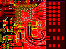
During mobile phone RF PCB development, engineers frequently encounter challenges such as:
- Signal loss caused by excessive routing length
- Impedance discontinuities
- Crosstalk between multiple wireless systems
- Ground plane interruptions
- Antenna detuning
- RF interference from switching power supplies
- Thermal effects on RF components
Addressing these issues early during PCB layout reduces debugging time and improves overall product performance.
Conclusion
Mobile phone RF PCB layout requires a balanced approach that considers electrical performance, mechanical constraints, thermal management, and manufacturing capability. Successful RF PCB design depends on careful optimization of component placement, impedance-controlled routing, grounding, power integrity, isolation, antenna integration, and EMI control.
As smartphones continue to support more wireless standards and higher operating frequencies, the demands on RF PCB design will continue to increase. Applying sound layout principles together with thorough DFM analysis and manufacturing validation helps improve signal integrity, reduce interference, and achieve reliable high-volume production.
