1. Introduction: Why PCB Footprint Accuracy Matters in Modern Electronics
In modern PCB design and electronic product development, accuracy at the earliest design stage directly determines manufacturing success, cost efficiency, and product reliability.
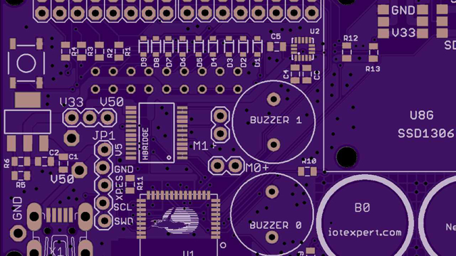
One of the most critical elements in PCB layout design is the PCB footprint, which defines the physical land pattern for electronic components such as ICs, resistors, capacitors, connectors, and RF modules.
As electronics move toward high-density interconnect (HDI), high-speed digital systems, and RF/microwave applications, manual footprint creation is no longer efficient or error-free. This is where an advanced PCB footprint generator becomes essential.
At KKPCB, footprint accuracy is considered a critical factor in ensuring high yield manufacturing, reliable assembly, and optimized PCB performance.
2. What Is an Advanced PCB Footprint Generator?
An advanced PCB footprint generator is a software-driven tool or system that automatically creates standardized and manufacturing-ready PCB footprints based on:
- Component datasheets
- IPC footprint standards (IPC-7351)
- Package types (BGA, QFN, LGA, SMD, etc.)
- Assembly and soldering constraints
It eliminates manual design errors and ensures consistency between schematic, layout, and manufacturing output.
3. Why PCB Footprint Generation Is Critical in PCB Design Workflow
3.1 Eliminating Human Design Errors
Manual footprint design often leads to:
- Incorrect pad spacing
- Misaligned solder pads
- Wrong component orientation
- Assembly incompatibility
An advanced footprint generator significantly reduces these risks by ensuring standardized, rule-based footprint creation.
3.2 Improving PCB Design Efficiency
In high-volume PCB design environments, speed is critical.
Footprint automation enables:
- Faster PCB library creation
- Reduced design iteration cycles
- Streamlined schematic-to-layout transition
- Rapid prototyping support
This is especially important for:
- Consumer electronics
- Automotive ECUs
- IoT device development
3.3 Ensuring Manufacturing Compatibility
PCB footprints must align with real-world manufacturing processes such as:
- SMT (Surface Mount Technology) assembly
- Reflow soldering profiles
- PCB fabrication tolerances
- Pick-and-place machine requirements
A footprint generator ensures compliance with DFM (Design for Manufacturing) and DFA (Design for Assembly) principles.
3.4 Enhancing Signal Integrity in High-Speed and RF Designs
In advanced PCB systems such as RF, microwave, and high-speed digital boards, footprint accuracy directly impacts electrical performance.
Incorrect footprint design can cause:
- Impedance mismatch
- Signal reflection
- Parasitic capacitance increase
- EMI issues
Proper footprint generation helps maintain:
- Controlled impedance routing
- Stable signal transitions
- Reduced parasitic effects
3.5 Supporting High-Density Interconnect (HDI) PCB Design
Modern PCB systems require extremely compact layouts.
Advanced footprint generators support:
- Micro BGA and fine-pitch components
- HDI via-in-pad structures
- Ultra-small SMD components (01005, 0201)
- Multi-layer routing optimization
This is essential for smartphones, wearables, and high-performance computing systems.
4. Key Features of an Advanced PCB Footprint Generator

A modern footprint generation system typically includes:
4.1 IPC-Compliant Library Creation
- Follows IPC-7351 standards
- Ensures global manufacturing compatibility
4.2 Automated Pad Dimension Calculation
- Based on component datasheets
- Adjusted for solder mask and assembly tolerances
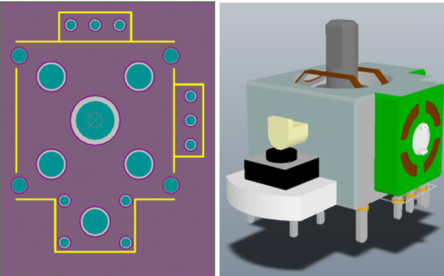
4.3 3D Footprint Modeling
- Mechanical collision checking
- Enclosure fit verification
- PCB-to-mechanical integration
4.4 Rule-Based Design Automation
- Standardized footprint templates
- Manufacturing rule validation
4.5 Multi-Format Export Support
- Compatible with major PCB design tools
- Easy integration into EDA workflows
5. Applications in Modern Electronics Manufacturing
Advanced PCB footprint generators are widely used in:
- Consumer electronics (smartphones, tablets)
- Automotive electronics (ECUs, ADAS systems)
- Industrial control systems
- RF and microwave communication modules
- Medical electronic devices
- IoT and wearable devices
Each of these applications requires high reliability, compact design, and precision assembly, making footprint automation essential.
6. KKPCB Approach to PCB Footprint and Layout Accuracy
At KKPCB, PCB footprint validation is integrated into the full manufacturing process:
- DFM (Design for Manufacturability) review
- DFA (Design for Assembly) optimization
- Pad and solder mask verification
- Component placement validation
- Assembly yield optimization
This ensures:
- High production yield
- Reduced assembly defects
- Stable electrical performance
- Reliable mass production scalability
7. Conclusion
The advanced PCB footprint generator is a critical tool in modern PCB design workflows, enabling engineers to achieve higher efficiency, greater accuracy, and improved manufacturability.
As electronic systems continue to evolve toward miniaturization, HDI structures, and high-speed performance, footprint automation becomes essential for reducing design risks and improving overall product reliability.
With strong engineering support and manufacturing expertise, KKPCB helps ensure that every PCB footprint translates into reliable, high-quality, and production-ready hardware.
