
With the rapid development of wireless communication, radar systems, IoT devices, automotive electronics, and satellite communication technologies, RF (Radio Frequency) PCB design has become increasingly important in modern electronic systems.
Unlike conventional digital PCBs, RF PCBs operate at high frequencies where even small variations in:
can significantly affect circuit performance.
A well-designed RF PCB must achieve:
- Stable impedance control
- Low signal loss
- Reduced electromagnetic interference (EMI)
- Reliable high-frequency transmission
- Consistent manufacturing performance
This article provides a comprehensive overview of RF PCB design principles, material selection, layout guidelines, manufacturing considerations, and common challenges.
1. What Is an RF PCB?

An RF PCB is a printed circuit board designed specifically for circuits operating at radio frequencies, typically from MHz to GHz ranges.
RF PCBs are used for applications involving:
- Wireless signal transmission
- High-frequency amplification
- Antenna systems
- Radar detection
- Microwave communication
Compared with standard PCBs, RF PCBs require stricter control over electrical characteristics.
2. Key Characteristics of RF PCB Design
2.1 Controlled Impedance
Impedance control is one of the most critical requirements in RF PCB design.
RF signals travel as electromagnetic waves along transmission lines. Any impedance mismatch can cause:
- Signal reflection
- Power loss
- Reduced transmission efficiency
Common RF impedance requirements include:
- 50Ω single-ended impedance
- 100Ω differential impedance
Factors affecting impedance include:
- Trace width
- Copper thickness
- Dielectric thickness
- Dielectric constant (Dk)
- Stack-up structure
2.2 Low Signal Loss
At high frequencies, signal loss becomes a major concern.
Loss sources include:
Dielectric Loss
Caused by energy absorption within the PCB material.
Reduced by using:
- Low-loss laminates
- Low dissipation factor materials
Conductor Loss
Related to:
- Copper roughness
- Skin effect
- Surface finish
Low-profile copper foil can help reduce high-frequency losses.
2.3 Electromagnetic Compatibility (EMC)
RF circuits are highly sensitive to electromagnetic interference.
Poor RF PCB design may cause:
- Signal interference
- Unwanted radiation
- Crosstalk
Effective EMC design requires:
- Proper grounding
- Shielding structures
- Controlled current return paths
3. RF PCB Material Selection
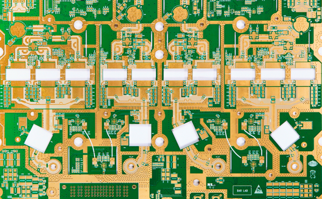
Material selection directly affects RF performance.
3.1 Rogers High-Frequency Materials
Materials such as:
- RO4003C
- RO4350B
- RO4835
are widely used in RF applications.
Advantages:
- Stable dielectric constant
- Low dielectric loss
- Good dimensional stability
Applications:
- RF modules
- Antenna boards
- Microwave circuits
3.2 PTFE-Based Materials
PTFE materials provide excellent high-frequency performance.
Advantages:
- Extremely low dielectric loss
- Excellent phase stability
Applications:
- Microwave circuits
- Aerospace communication systems
Challenges:
- More complex processing
- Higher manufacturing cost
3.3 High-Performance FR-4
Advanced FR-4 materials may be used for lower-frequency RF applications.
Advantages:
- Cost-effective
- Easy manufacturing
Limitations:
- Higher dielectric loss compared with specialized https://www.kkpcba.com/pcb-materials/RF materials
4. RF PCB Stack-Up Design
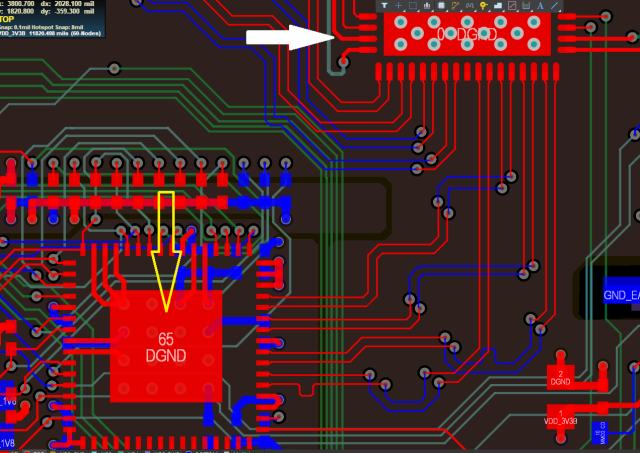
A proper stack-up is essential for RF performance.
4.1 Reference Plane Design
RF transmission lines require stable reference planes.
Benefits:
- Controlled impedance
- Reduced noise
- Improved return paths
Ground planes should be:
- Continuous
- Properly connected
- Free from unnecessary splits
4.2 Layer Arrangement
Common RF PCB stack-up considerations:
Signal Layer
Used for:
- RF traces
- Transmission lines
Ground Layer
Provides:
- Return path
- Shielding
Power Layer
Supports:
- Stable power delivery
5. RF PCB Routing Guidelines
5.1 Keep RF Signal Paths Short
Long RF traces increase:
- Insertion loss
- Signal attenuation
Design recommendations:
- Minimize unnecessary routing length
- Avoid sharp direction changes
5.2 Use Controlled Transmission Lines
Common RF transmission structures include:
Microstrip Line
A conductor trace above a ground plane.
Advantages:
- Simple structure
- Easy fabrication
Applications:
- RF modules
- Antenna connections
Stripline
A conductor trace between two reference planes.
Advantages:
- Better shielding
- Improved electromagnetic control
Applications:
- High-performance RF systems
5.3 Avoid Sharp Corners
Sharp corners may cause:
- Impedance discontinuity
- Signal reflection
Recommended methods:
- Use curved traces
- Use 45-degree routing
5.4 Maintain Proper Trace Spacing
Insufficient spacing may increase:
- Crosstalk
- Electromagnetic coupling
Spacing should consider:
- Frequency
- Trace width
- Layer structure
6. RF PCB Grounding Design
Grounding is one of the most important aspects of RF PCB design.
6.1 Maintain Continuous Ground Planes
A continuous ground plane provides:
- Stable return path
- Reduced EMI
- Improved signal integrity
Avoid:
- Splitting RF return paths
- Excessive plane gaps
6.2 Via Stitching
Ground vias are often placed around RF traces and circuits.
Benefits:
- Improved shielding
- Reduced electromagnetic radiation
- Better grounding performance
6.3 Separate RF and Digital Circuits
Mixed-signal designs require careful isolation.
Design methods:
- Separate sensitive RF areas
- Control return current paths
- Use filtering and shielding
7. RF PCB Antenna Design Considerations
For wireless products, antenna performance depends heavily on PCB design.
Important factors include:
- Antenna placement
- Ground clearance
- Dielectric properties
- Matching network design
Poor layout may result in:
- Reduced antenna efficiency
- Signal range reduction
8. RF PCB Power Integrity Design
RF circuits require stable power supplies.
Power problems may cause:
- Noise generation
- Frequency instability
- Reduced signal quality
Design methods include:
- Proper decoupling capacitor placement
- Short power paths
- Low-inductance connections
9. RF PCB Manufacturing Considerations
RF performance depends heavily on manufacturing accuracy.
9.1 Material Processing Control
Important controls include:
- Dielectric thickness
- Copper thickness
- Lamination parameters
Variations can affect:
- Impedance accuracy
- Signal loss
9.2 Impedance Testing
RF PCBs commonly require impedance verification.
Methods include:
- TDR testing
- Coupon testing
Typical impedance tolerance requirements may include:
- ±5%
- ±8%
depending on application requirements.
9.3 Surface Finish Selection
Surface finish affects RF performance.
Considerations include:
- Copper loss
- Reliability
- Solderability
Common finishes:
- ENIG
- ENEPIG
10. Common RF PCB Design Challenges
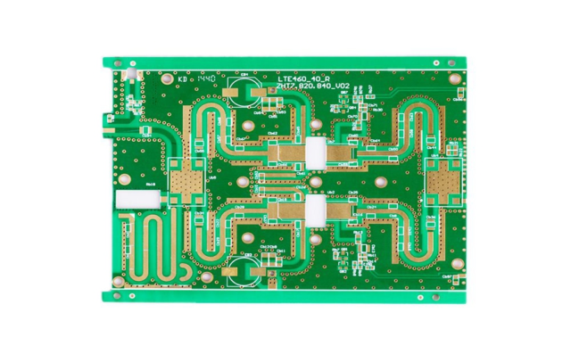
10.1 Impedance Mismatch
Causes:
- Incorrect trace geometry
- Material variation
- Stack-up errors
Effects:
- Reflection
- Signal loss
10.2 Excessive Signal Loss
Causes:
- High-loss materials
- Long transmission paths
- Poor routing
Solutions:
- Use low-loss materials
- Optimize routing
10.3 EMI Problems
Causes:
- Poor grounding
- Improper shielding
- Return path interruption
Solutions:
- Improve grounding
- Add shielding structures
10.4 Thermal Issues
RF power circuits may generate heat.
Solutions:
- Thermal vias
- Copper optimization
- Proper component placement
11. Applications of RF PCBs
Wireless Communication
Applications:
- 5G equipment
- Wireless modules
- Base stations
Requirements:
- High-frequency stability
- Low signal loss
Automotive Radar
Applications:
- 24GHz radar
- 77GHz radar systems
Requirements:
- Precise impedance control
- High-frequency reliability
Aerospace and Satellite Systems
Applications:
- Communication satellites
- Navigation systems
Requirements:
- Phase stability
- Extreme reliability
IoT Devices
Applications:
- Wireless sensors
- Smart devices
Requirements:
- Compact size
- Low power consumption
12. RF PCB Design Checklist
Before production, engineers should verify:
Material
- Appropriate dielectric material selected
- Stable Dk/Df values confirmed
Stack-Up
- Controlled impedance structure
- Continuous reference planes
Layout
- Short RF paths
- Proper trace spacing
- Reduced discontinuities
Grounding
- Complete return paths
- Proper via stitching
Manufacturing
- Impedance testing completed
- Material processing controlled
- DFM review performed
Conclusion
RF PCB design requires a combination of electrical, mechanical, and manufacturing considerations.
Successful RF PCB development depends on controlling:
- Impedance
- Signal loss
- Material properties
- Grounding structures
- Manufacturing tolerances
From wireless communication systems and automotive radar to satellite electronics and IoT devices, RF PCB technology provides the foundation for reliable high-frequency signal transmission.
With proper material selection, optimized layout, and advanced manufacturing control, RF PCBs can achieve excellent performance and long-term reliability in demanding applications.
