HomeTag

design - KKPCB

Advantages and Applications of Double-Sided PCB

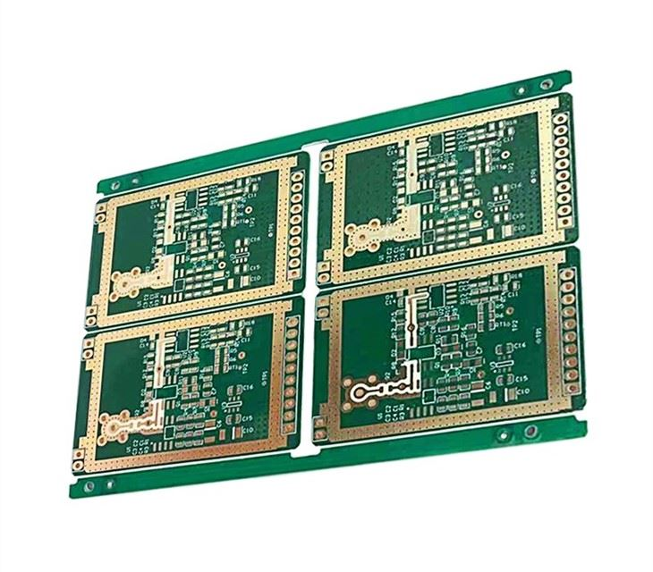
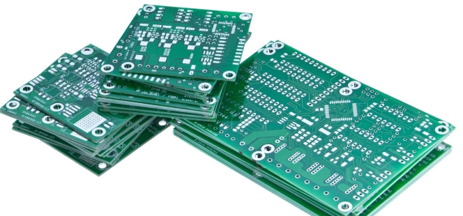
A double-sided PCB (Double-Sided Printed Circuit Board) is a type of circuit board with copper layers on both the top and bottom sides, allowing electrical connections and component placement on both surfaces. Compared with single-sided PCBs, double-sided PCBs provide significantly higher routing density and greater design flexibility. Compared with multilayer PCBs, they offer a more...
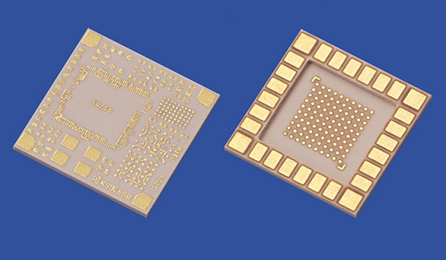
Ceramic Substrate

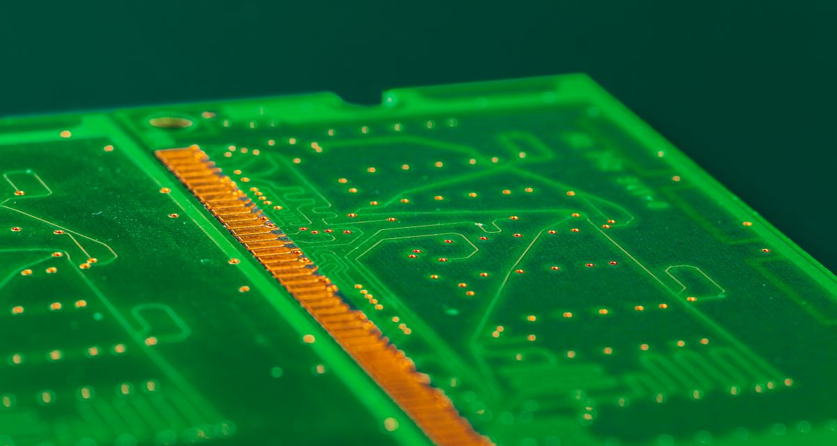
With the continuous development of power electronics, RF communication, semiconductor devices, and high-reliability electronic systems, traditional PCB materials are facing increasing challenges in applications requiring high thermal conductivity, electrical insulation, and extreme environmental stability. Ceramic substrates have become an important material solution for advanced electronic applications due to their excellent thermal performance, mechanical stability, and...

RO4003C/RO4350B/RO4835 Laminates Quick Reference Processing Guide

With the increasing demand for higher frequency communication, advanced radar systems, and high-speed electronic applications, PCB materials must provide stable electrical performance while maintaining reliable manufacturability. RO4003C™, RO4350B™, and RO4835™ laminates are high-frequency circuit materials developed for applications requiring low signal loss, stable dielectric properties, and improved thermal performance. These materials combine ceramic-filled hydrocarbon resin...

RO4835™ Laminate Data Sheet High Frequency PCB Materials

As electronic systems continue moving toward higher frequencies, faster signal transmission, and more demanding operating environments, PCB material selection has become a critical factor affecting product performance. For RF, microwave, automotive radar, and high-speed communication applications, conventional FR-4 materials may not always provide sufficient electrical stability due to higher dielectric loss and variations in dielectric...

Key Grounding Techniques in Electronic Design

Grounding is one of the most fundamental elements in electronic system design. A well-designed grounding structure provides a stable reference potential, ensures reliable current return paths, reduces electrical noise, and improves overall system performance. As electronic products continue developing toward higher operating frequencies, faster data transmission, and increased integration, grounding design has become more challenging....

Balanced PCB Stack-Up Design Method

As electronic products continue evolving toward higher integration, faster signal transmission, and more compact designs, PCB stack-up design has become a critical factor affecting electrical performance and manufacturing reliability. A PCB stack-up is not simply an arrangement of copper layers and dielectric materials. It determines: Signal integrity Power distribution performance Electromagnetic compatibility (EMC) Mechanical stability...

PCB Design Principles for Single-Chip Microcontroller Control Boards

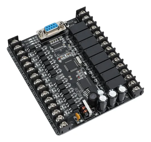
Single-chip microcontroller (MCU) control boards are widely used in industrial automation, consumer electronics, automotive systems, medical devices, smart sensors, and embedded control applications. Although MCU-based systems are relatively compact compared with complex computing platforms, their PCB design still requires careful engineering consideration. Factors such as power stability, clock signal quality, reset reliability, electromagnetic compatibility (EMC),...

How to Reduce Circuit Board Noise

As electronic products continue to become faster, smaller, and more integrated, circuit board noise has become a major challenge in PCB design. High-speed processors, switching power supplies, wireless communication modules, and sensitive analog circuits all generate unwanted electrical noise that can affect system performance. Excessive PCB noise may result in: Signal distortion Communication errors Measurement...

Guide to Restoring Circuit Diagrams from Physical PCBs

In electronic product development, maintenance, and redesign projects, engineers may encounter situations where the original circuit documents are unavailable or incomplete. A common solution is to restore the circuit diagram from an existing physical PCB. PCB reverse engineering, also known as schematic reconstruction, involves analyzing the physical circuit board structure, identifying components and connections, and...

Can Pull-up Resistors Be Used on SPI Lines?

The SPI (Serial Peripheral Interface) is a widely used synchronous communication protocol in embedded systems, commonly applied for communication between: Microcontrollers (MCUs) Sensors Memory devices ADC/DAC converters Display controllers Communication modules Unlike protocols such as I²C, which use open-drain signaling and require pull-up resistors by design, SPI typically uses push-pull drivers. This leads to a...