
In electronic product development, maintenance, and redesign projects, engineers may encounter situations where the original circuit documents are unavailable or incomplete. A common solution is to restore the circuit diagram from an existing physical PCB.
PCB reverse engineering, also known as schematic reconstruction, involves analyzing the physical circuit board structure, identifying components and connections, and rebuilding the corresponding schematic diagram.
This process is widely used in:
- Legacy product maintenance
- Equipment upgrades
- Failure analysis
- Functional replication
- Prototype improvement
- Hardware documentation recovery
However, restoring a PCB schematic is not simply copying visible traces. It requires a systematic approach combining electrical analysis, PCB knowledge, and verification methods.
1. Why Restore Circuit Diagrams from Physical PCBs?
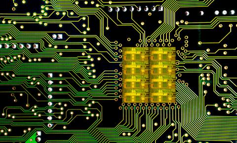
A complete schematic diagram is essential for understanding circuit operation and supporting future development.
Common reasons for PCB schematic restoration include:
Missing Design Files
Many older products may lack:
- Original schematic files
- PCB layout files
- Component libraries
- Design documentation
Restoring the schematic allows engineers to continue product development and maintenance.
Product Improvement and Redesign
A recovered schematic helps engineers:
- Analyze existing circuits
- Replace obsolete components
- Improve performance
- Optimize manufacturing processes
Fault Diagnosis
A schematic provides visibility into:
- Signal paths
- Power networks
- Component relationships
This makes troubleshooting more efficient.
2. Preparation Before PCB Reverse Engineering
Before starting schematic restoration, engineers should collect as much information as possible.
Required materials may include:
- Physical PCB sample
- High-resolution PCB images
- Component datasheets
- Multimeter
- Microscope
- PCB inspection tools
- CAD software
Inspect the PCB Structure
Initial inspection should identify:
- PCB layer count
- Board dimensions
- Component locations
- Connector types
- Major functional blocks
For multilayer PCBs, internal copper layers cannot be directly observed, making tracing more challenging.
3. Step One: Identify PCB Components
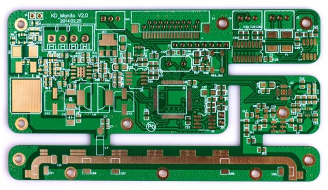
Component identification is the first stage of schematic reconstruction.
Engineers should record:
- Reference designators
- Package types
- Marking codes
- Component values
- Manufacturer information
Passive Components
Common components include:
- Resistors
- Capacitors
- Inductors
- Diodes
Their values may be identified through:
- Component markings
- Measurement tools
- Circuit analysis
Integrated Circuits (ICs)
IC identification requires checking:
- Part numbers
- Package types
- Pin configurations
- Datasheets
Understanding IC functions helps determine circuit relationships.
Examples:
- Power management ICs
- Microcontrollers
- Amplifiers
- Communication chips
4. Step Two: Analyze PCB Layers and Copper Connections
After component identification, the next step is mapping electrical connections.
Single-Layer and Double-Layer PCBs
These boards are relatively easier to analyze because traces are visible.
The process includes:
- Following copper traces
- Recording connection points
- Identifying vias
- Mapping component relationships
Multilayer PCB Challenges
Modern PCBs often contain:
- Multiple signal layers
- Internal power planes
- Buried vias
- Blind vias
These structures make direct tracing difficult.
Additional methods may include:
- X-ray inspection
- Cross-section analysis
- CT scanning
5. Step Three: Create the Schematic Diagram
After collecting connection information, engineers can begin schematic reconstruction.
The schematic should include:
- Component symbols
- Reference designators
- Net connections
- Power rails
- Signal paths
Start with Functional Blocks
Instead of drawing the entire circuit immediately, divide the PCB into sections:
- Power supply circuit
- Control circuit
- Communication interface
- Analog processing circuit
- Output driver circuit
This approach makes complex boards easier to understand.
Reconstruct Power Networks First
Power circuits are usually easier to identify and provide a foundation for the rest of the schematic.
Important power sections include:
- Input protection
- Voltage conversion
- Filtering circuits
- Ground connections
Trace Signal Paths
After power reconstruction, analyze:
- Clock signals
- Communication lines
- Control signals
- Analog paths
Understanding signal flow helps confirm circuit functions.
6. Step Four: Verify the Reconstructed Schematic
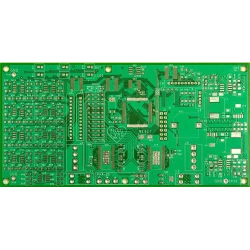
Verification is a critical step because incorrect connections can lead to design errors.
Electrical Testing
Common verification methods include:
- Continuity testing
- Resistance measurement
- Voltage measurement
- Signal waveform analysis
These tests help confirm actual PCB connections.
Compare with Component Datasheets
Datasheet comparison helps verify:
- IC pin connections
- Power requirements
- Peripheral components
- Typical application circuits
Functional Testing
If possible, test the original PCB operation and compare expected behavior with the reconstructed schematic.
This helps identify:
- Missing connections
- Incorrect component values
- Hidden design functions
7. Common Challenges in PCB Schematic Restoration
Hidden Internal Layers
Multilayer boards may contain complex internal routing that cannot be observed visually.
Solutions include:
- PCB scanning
- X-ray inspection
- Professional reverse engineering services
Unknown Components
Some components may have:
- Unclear markings
- Customized parts
- Obsolete models
Engineers may need to identify alternatives through electrical characteristics.
Complex High-Speed Circuits
High-speed and RF circuits require special attention because small errors can affect:
- Signal integrity
- Impedance matching
- Timing performance
For these circuits, schematic restoration should also consider:
- Transmission line structures
- Controlled impedance requirements
- Grounding design
8. Tools Used for PCB Circuit Diagram Restoration
PCB Design Software
Common tools include:
- Altium Designer
- Cadence OrCAD
- KiCad
- PADS
These tools allow engineers to recreate:
- Schematics
- PCB layouts
- Component libraries
Measurement Equipment
Useful equipment includes:
- Digital multimeter
- Oscilloscope
- Logic analyzer
- Network analyzer
Advanced Inspection Equipment
For complex boards:
- X-ray inspection systems
- Automatic optical inspection (AOI)
- 3D imaging systems
can provide additional visibility.
9. Considerations for High-Density PCB Reverse Engineering
Modern electronic products often use:
- HDI technology
- Microvias
- Fine-pitch components
- High-layer-count PCBs
These designs require more advanced analysis methods.
Important considerations include:
- Via structure identification
- Layer stack-up analysis
- Impedance evaluation
- Manufacturing process understanding
10. Applications of PCB Schematic Restoration
PCB schematic reconstruction is commonly applied in:
- Industrial equipment repair
- Automotive electronics
- Medical devices
- Communication systems
- Consumer electronics
- Legacy product upgrades
- Hardware documentation recovery
It helps extend product lifecycle and supports future engineering improvements.
Conclusion
Restoring a circuit diagram from a physical PCB is a systematic process that combines visual inspection, component identification, electrical tracing, schematic drawing, and functional verification.
The key steps include:
- Inspecting the PCB structure
- Identifying components and functions
- Mapping electrical connections
- Creating schematic diagrams
- Verifying the reconstructed design
For simple boards, manual tracing may be sufficient. However, complex multilayer, high-speed, or RF PCBs require advanced inspection techniques and deeper engineering analysis.
With proper methods and tools, PCB schematic restoration can provide valuable design information, support product maintenance, and enable future optimization of electronic systems.
