
A double-sided PCB (Double-Sided Printed Circuit Board) is a type of circuit board with copper layers on both the top and bottom sides, allowing electrical connections and component placement on both surfaces.
Compared with single-sided PCBs, double-sided PCBs provide significantly higher routing density and greater design flexibility. Compared with multilayer PCBs, they offer a more cost-effective solution for electronic products that require moderate circuit complexity.
Due to their balance between performance, manufacturing difficulty, and cost, double-sided PCBs are widely used in:
- Industrial control equipment
- Consumer electronics
- Power management systems
- Automotive electronics
- Instrumentation equipment
- Embedded control systems
A properly designed double-sided PCB can achieve reliable electrical performance while maintaining efficient manufacturing and assembly processes.
1. What Is a Double-Sided PCB?
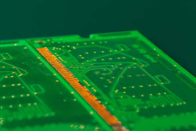
A double-sided PCB consists of:
- Top copper layer
- Bottom copper layer
- Insulating substrate
- Through-hole vias
- Solder mask
- Surface finish
Unlike a single-sided PCB where all traces are located on one side, double-sided PCBs allow circuits to be routed on both sides.
The two copper layers are electrically connected through:
- Plated through holes (PTH)
- Vias
This structure increases routing space and enables more complex circuit designs.
2. Structure of Double-Sided PCBs
A typical double-sided PCB structure includes:
2.1 Copper Layers
Copper layers provide:
- Signal transmission paths
- Power distribution
- Ground connections
The copper thickness can be selected according to application requirements.
Common copper thickness options include:
- 1 oz copper
- 2 oz copper
- Heavy copper designs for higher current applications
2.2 Substrate Material
The substrate provides mechanical support and electrical insulation.
Common materials include:
FR-4
The most widely used PCB material.
Advantages:
- Good mechanical strength
- Stable electrical properties
- Cost-effective
High-Tg FR-4
Suitable for:
- High-temperature environments
- Industrial applications
Advantages:
- Better thermal stability
- Improved reliability
2.3 Via Structures
Vias connect circuits between the top and bottom layers.
Common types include:
- Through vias
- Blind vias
- Buried vias (mainly used in multilayer PCBs)
For standard double-sided PCBs, through-hole vias are most common.
3. Advantages of Double-Sided PCBs
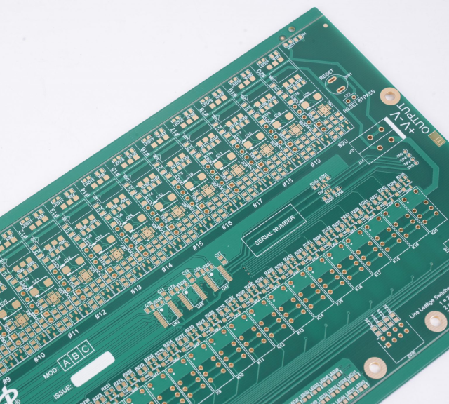
3.1 Higher Wiring Density
One of the biggest advantages of double-sided PCBs is increased routing space.
Compared with single-sided PCBs:
- More signal paths can be created
- Complex circuits can be integrated
- Board size can be reduced
This makes them suitable for products requiring moderate circuit complexity.
3.2 More Flexible Component Placement
Components can be mounted on:
- Top side
- Bottom side
This provides greater design flexibility.
Benefits include:
- Optimized layout
- Reduced board size
- Improved signal routing
3.3 Better Electrical Performance
Double-sided PCBs provide improved control over:
- Signal paths
- Ground connections
- Power distribution
A dedicated bottom layer can be used for:
- Ground routing
- Power distribution
- Signal return paths
This helps reduce:
- Electrical noise
- Signal interference
3.4 Improved Cost Performance
Compared with multilayer PCBs, double-sided PCBs offer:
- Lower manufacturing cost
- Simpler production process
- Shorter fabrication cycle
They are a practical choice when a single-sided PCB cannot meet routing requirements but a multilayer PCB is unnecessary.
3.5 Suitable for Automated Assembly
Double-sided PCBs support modern assembly processes including:
- SMT (Surface Mount Technology)
- THT (Through-Hole Technology)
Advantages:
- High assembly efficiency
- Better component utilization
- Flexible production options
4. Manufacturing Process of Double-Sided PCBs
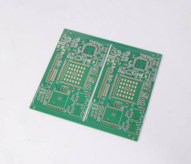
The manufacturing process includes several key steps.
4.1 Material Preparation
The process begins with copper-clad laminate preparation.
Steps include:
- Cutting materials
- Surface cleaning
- Layer preparation
4.2 Inner Circuit Pattern Formation
Although double-sided PCBs do not have inner layers, both copper surfaces require circuit pattern processing.
The process includes:
- Photoresist coating
- Exposure
- Development
- Etching
The required circuit patterns are formed on both sides.
4.3 Drilling
Holes are drilled according to design requirements.
Functions include:
- Component mounting
- Electrical connection between layers
Important parameters:
- Hole diameter
- Position accuracy
- Aspect ratio
4.4 Through-Hole Plating
After drilling, copper plating is applied inside the holes.
This creates electrical connections between:
- Top copper layer
- Bottom copper layer
Reliable plating is essential for long-term PCB performance.
4.5 Solder Mask and Surface Finish
The solder mask protects copper traces.
Surface finishes may include:
- HASL
- ENIG
- OSP
Selection depends on:
- Component type
- Assembly process
- Reliability requirements
5. Applications of Double-Sided PCBs
5.1 Industrial Control Systems
Double-sided PCBs are widely used in:
- PLC controllers
- Automation equipment
- Industrial monitoring systems
Reasons include:
- Good reliability
- Moderate complexity support
- Cost efficiency
5.2 Power Electronics
Applications include:
- Power supply boards
- Motor controllers
- Battery management systems
Design considerations:
- Current carrying capability
- Thermal management
- Copper thickness selection
5.3 Consumer Electronics
Used in products such as:
- Home appliances
- Audio equipment
- Smart devices
Advantages:
- Compact size
- Efficient production
- Affordable manufacturing
5.4 Automotive Electronics
Applications include:
- Vehicle control modules
- Sensor control boards
- Dashboard electronics
Requirements:
- Mechanical reliability
- Temperature resistance
- Long operating lifetime
5.5 Communication Equipment
Double-sided PCBs can be used in:
- Wireless modules
- Signal control boards
- Embedded communication devices
Important considerations:
- Signal integrity
- EMI control
- Grounding design
6. Design Considerations for Double-Sided PCBs
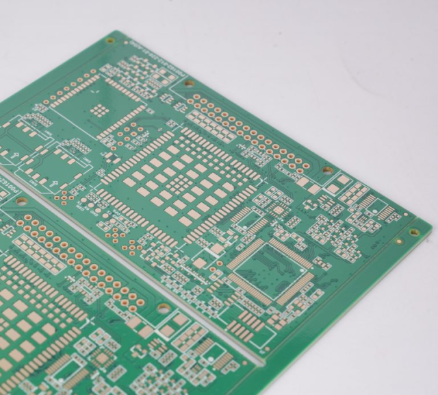
6.1 Component Placement Planning
Good placement improves:
- Routing efficiency
- Thermal distribution
- Assembly quality
Recommended practices:
- Place critical components first
- Separate sensitive circuits from noisy circuits
- Consider heat-generating components
6.2 Grounding Design
Ground design affects:
- Noise performance
- Signal quality
- System stability
Recommended methods:
- Use large ground areas
- Minimize ground return paths
- Avoid unnecessary signal loops
6.3 Trace Width and Current Capacity
Trace width should match current requirements.
Factors include:
- Copper thickness
- Operating current
- Temperature rise
High-current circuits may require:
- Wider traces
- Copper pours
- Thicker copper layers
6.4 Thermal Management
Heat management should be considered for:
- Power devices
- Regulators
- Motor drivers
Solutions include:
- Enlarged copper areas
- Thermal vias
- Improved airflow paths
7. Limitations of Double-Sided PCBs
Although double-sided PCBs offer many advantages, they also have limitations.
7.1 Limited Routing Density
Compared with multilayer PCBs:
- Routing space is lower
- Complex circuits may become difficult
7.2 More Difficult Signal Control
For high-speed applications, double-sided PCBs may face challenges in:
- Controlled impedance
- Signal return paths
- EMI management
7.3 Limited Space for Advanced Designs
Applications requiring:
- High layer counts
- High-density interconnects
- Complex power distribution
may require multilayer PCB solutions.
8. Double-Sided PCB vs Single-Sided PCB vs Multilayer PCB
| PCB Type | Advantages | Typical Applications |
|---|---|---|
| Single-Sided PCB | Low cost, simple manufacturing | Basic electronic products |
| Double-Sided PCB | Better routing density, balanced cost | Industrial controls, embedded systems |
| Multilayer PCB | High density, advanced performance | High-speed, complex electronic systems |
Conclusion
Double-sided PCBs provide an effective balance between design flexibility, manufacturing complexity, and cost.
Their main advantages include:
- Increased wiring density
- Flexible component placement
- Improved electrical performance
- Compatibility with SMT and THT assembly
- Cost-effective production
Although they may not replace multilayer PCBs in highly complex or high-speed applications, double-sided PCBs remain an important solution for many electronic products requiring reliable performance and economical manufacturing.
With proper design considerations including grounding, thermal management, trace optimization, and DFM analysis, double-sided PCBs can achieve excellent reliability and production efficiency.
