
Why PCB Material Characterization Matters at High Frequencies
The electrical properties of a PCB material can be characterized using several different measurement techniques. Some methods directly evaluate the dielectric material using specialized fixtures, while others characterize the material through an actual circuit structure.
This distinction becomes increasingly important as PCB operating frequencies move from conventional microwave frequencies into the millimeter-wave range.
Material datasheets commonly provide values for dielectric constant (Dk) and dissipation factor (Df). However, engineers may sometimes find that the Dk extracted from a circuit test does not exactly match the Dk reported from a fixture-based material test.
This does not necessarily mean that one measurement is incorrect.
Instead, the difference can result from the measurement method, electromagnetic field distribution, PCB fabrication process, copper geometry, surface roughness, and material anisotropy.
For engineers designing 5G mmWave PCB, 77 GHz radar PCB, RF modules, high-speed digital PCB, and multilayer RF PCB, understanding these differences is essential for selecting the correct material data and building accurate simulation models.
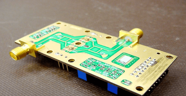
Fixture-Based vs. Circuit-Based PCB Material Testing
There are two broad approaches to high-frequency PCB material characterization.
Fixture-Based Material Measurement
Fixture-based testing directly characterizes a material sample using a controlled measurement structure.
This approach is commonly used to determine dielectric properties such as Dk and Df for material datasheets.
One advantage is that the test does not directly depend on many PCB manufacturing variables.
However, fixture-based measurements can still be affected by:
- Fixture alignment
- Air gaps
- Coupling conditions
- Mechanical tolerances
- Sample preparation
- Field distribution
The measured value is therefore associated with a specific test method and should not automatically be treated as an absolute material constant under every circuit configuration.
Circuit-Based Measurement
Circuit-based characterization uses an actual RF structure to extract electrical properties.
Common PCB test circuits include:
- Ring resonators
- Transmission lines
- Different-length transmission lines
- Patch antennas
- 180-degree hybrid couplers
- Delay lines
- Resonant structures
The major advantage is that the test circuit can more closely represent the actual PCB application.
However, circuit-based testing introduces additional variables from PCB fabrication.
These may include:
- Trace width variation
- Copper thickness variation
- Etching profile
- Copper surface roughness
- Surface finish
- Dielectric thickness
- Layer registration
- Via geometry
This is why PCB Dk testing using a circuit structure can produce a value that differs from a material datasheet.
Why Dk Values Can Be Different Between Test Methods
A useful way to understand this issue is to consider the difference between a material measurement and a manufactured circuit measurement.
A fixture primarily evaluates the dielectric material under a controlled test configuration.
A circuit test evaluates the interaction between:
Material + Copper + Geometry + Fabrication + Electromagnetic Field
Therefore, if a circuit-derived Dk changes from one PCB manufacturing batch to another, the variation may not necessarily represent a change in the intrinsic dielectric material.
For example, two ring resonators may use the same laminate design but be manufactured at different times.
If one circuit has slightly different copper thickness or trace geometry, its electromagnetic field distribution can change.
The extracted Dk may therefore change even though the nominal PCB material remains the same.
This distinction is particularly important when characterizing millimeter-wave PCB materials, where small physical variations can become electrically significant.
Material Anisotropy and Dk Measurement
Most PCB materials are not perfectly isotropic.
Their dielectric properties can differ along the three principal axes:
- X-axis
- Y-axis
- Z-axis
This is known as dielectric anisotropy.
For multilayer PCB applications, the Z-axis Dk is particularly relevant because many RF structures interact with the dielectric in the thickness direction.
Different test methods can generate different electromagnetic field orientations. Consequently, the measured Dk can vary depending on how the electric field interacts with the material.
Engineers should therefore confirm:
Which Dk was measured?
At what frequency?
Using which test method?
In which field direction?
For which material construction and thickness?
These questions are important when using material datasheet values for RF simulation or impedance calculation.
Why Ring Resonators Can Become Challenging at mmWave Frequencies
Ring resonators have been used for PCB material characterization for many years.
They are useful because their resonant frequency can be related to the effective dielectric properties of the transmission structure.
However, as frequency increases into the millimeter-wave range, extracting material properties from ring resonators becomes more sensitive to circuit imperfections.
The fundamental reason is wavelength.
At lower frequencies, the wavelength is relatively large compared with small PCB manufacturing variations.
At millimeter-wave frequencies, the wavelength becomes much shorter.
Consequently, small changes in:
- Trace width
- Coupling gap
- Copper thickness
- Etching profile
- Surface roughness
- Dielectric thickness
can represent a more significant fraction of the electromagnetic structure.
A manufacturing variation that has little measurable effect at a lower frequency may therefore influence the RF response at 60 GHz or 77 GHz.
Coupling Gap Effects in Ring Resonator Testing
Many ring resonators use gap coupling.
The coupling gap can influence the resonant response and therefore affect the extraction of Dk.
At millimeter-wave frequencies, the coupling structure becomes particularly sensitive to manufacturing variation.
Consider two nominally identical ring resonators.
If one has slightly thicker copper, the geometry of the coupling region changes.
The distribution of fringing electromagnetic fields can also change.
Because air has a very low dielectric constant, an increase in the portion of the electric field extending into air can reduce the effective dielectric constant extracted from the circuit.
The resulting Dk value may therefore reflect the combined effect of material and circuit manufacturing, rather than the intrinsic Dk of the laminate alone.
This is one reason why a circuit-derived Dk should always be interpreted in the context of the test structure and manufacturing process.
Etching Profile and Trace Geometry
PCB etching does not always produce a perfectly rectangular copper conductor.
Depending on the fabrication process, the cross-section may have a trapezoidal profile.
The actual trace width at the top and bottom of the copper can therefore differ.
At conventional frequencies, this variation may have limited impact.
At millimeter-wave frequencies, however, the conductor profile can influence electromagnetic field distribution and impedance.
As a result, two boards manufactured using the same nominal Gerber geometry can show slightly different RF characteristics.
For accurate millimeter-wave PCB testing, the actual manufactured geometry should be considered whenever possible.
Copper Roughness and High-Frequency PCB Loss
Copper surface roughness is another important variable in high-frequency PCB material characterization.
The relevant surface is the copper interface that contacts the dielectric during laminate construction.
As frequency increases, current distribution becomes concentrated near the conductor surface. Surface roughness can increase the effective electrical path and contribute to conductor loss.
Therefore, copper roughness can affect:
- Insertion loss
- Phase response
- Propagation characteristics
- Effective transmission-line behavior
- RF repeatability
The roughness of copper foil is also not perfectly constant between production lots.
Even when the same nominal copper type is used, normal batch-to-batch variation can occur.
In a microstrip structure, the copper roughness on the signal layer and reference-plane side may also differ.
For this reason, copper roughness should be included in high-frequency PCB material evaluation, especially for 5G mmWave and 77 GHz applications.
Why Test Method Selection Depends on the Application
There is no single test method that is best for every PCB material evaluation.
The correct approach depends on the purpose of the measurement.
If the objective is to determine whether a material will perform consistently in mass-produced PCBs, the test structure should ideally represent the actual production circuit as closely as practical.
For example, a 77 GHz automotive radar PCB should be evaluated using a test structure that reflects the relevant transmission-line geometry, material stackup, copper configuration, and manufacturing process.
If the objective is to compare several materials for future projects, using the same controlled test method for every material may provide a more consistent comparison.
However, even this approach has limitations.
Different PCB materials may require different fabrication processes.
A process that is ideal for one material may not be optimal for another.
Therefore, a completely identical circuit fabrication process does not necessarily guarantee a perfectly fair comparison.
The test method, material, circuit structure, and manufacturing process must be interpreted together.
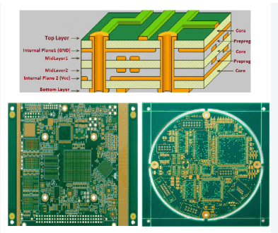
Common PCB Test Circuits for RF Material Characterization
Different circuit structures provide different types of information.
Ring Resonator
Ring resonators are commonly used for dielectric characterization and resonant-frequency analysis.
They can be useful for Dk extraction but become increasingly sensitive to coupling geometry and fabrication tolerances at millimeter-wave frequencies.
Transmission Line
Transmission-line structures can be designed with different lengths to evaluate propagation loss and phase behavior.
They are particularly useful when engineers want to understand the performance of a material in a structure that resembles an actual RF interconnect.
Delay Line
Delay lines can be used to evaluate signal propagation characteristics and phase delay.
They can be useful for high-speed digital and RF applications where propagation time and phase stability are important.
Patch Antenna
Patch antennas provide a way to evaluate the material within an antenna structure.
They can be particularly relevant when the target application is an RF antenna PCB, 5G antenna PCB, or millimeter-wave antenna module.
180-Degree Hybrid Coupler
Hybrid structures can be used to characterize amplitude and phase behavior in RF circuits.
They are useful for evaluating material performance in more complex microwave structures.
Recommended Test Strategy for 5G and 77 GHz PCB Materials
For advanced applications, the test method should be selected according to the final product requirements.
For example:
| Application | Recommended Evaluation Focus |
|---|---|
| High-speed digital PCB | Dk, Df, impedance, propagation delay |
| RF PCB | Dk, Df, insertion loss, phase |
| 5G PCB | Dk stability, Df, copper roughness, impedance |
| 5G mmWave PCB | Low-loss material + transmission-line behavior |
| 60 GHz PCB | Circuit geometry + dielectric loss |
| 77 GHz radar PCB | Insertion loss, phase stability, impedance, surface roughness |
| Multilayer RF PCB | Dk/Df + stackup + lamination + registration |
| High-layer-count PCB | Material compatibility + dimensional stability |
The important point is that material datasheet values should be matched to the measurement method used in the actual engineering model.
Engineering DFM Considerations for High-Frequency PCB Testing
When a PCB test coupon is used to characterize RF materials, the coupon itself must be manufactured with appropriate control.
Important DFM factors include:
Trace Width Control
The designed transmission-line width must be achievable with repeatable etching.
Copper Thickness Control
Copper thickness affects impedance, conductor loss, and coupling geometry.
Dielectric Thickness
The finished dielectric thickness should be considered rather than relying only on nominal laminate or prepreg thickness.
Copper Roughness
The selected copper foil and surface profile should be documented for demanding RF applications.
Coupling Gap
For resonator structures, coupling gaps should be large enough to remain within the manufacturer’s repeatable process capability.
Surface Finish
The final surface finish can alter the conductor structure and should be considered when interpreting high-frequency test results.
Layer Registration
Multilayer test coupons should maintain accurate alignment between RF traces and reference planes.
Material Lot Control
For production correlation, material lot information should be recorded so that electrical variations can be compared with material and manufacturing data.
KKPCB Approach to High-Frequency PCB Material Evaluation
For customers developing millimeter-wave PCB, 77 GHz radar PCB, 5G mmWave PCB, RF module PCB, and high-speed multilayer PCB, KKPCB can evaluate material and manufacturing requirements before production.
The engineering review can include:
- Material selection
- Dk and Df requirements
- RF stackup review
- Transmission-line structure
- Impedance requirements
- Copper thickness
- Copper roughness
- Finished dielectric thickness
- Etching capability
- Via structure
- Layer registration
- RF test coupon design
- Prototype fabrication
- Production DFM
The goal is to ensure that the material data used during simulation is reasonably aligned with the actual manufactured PCB.
For demanding RF projects, this connection between simulation data and production reality is critical.
A PCB model may use an ideal Dk value, but the final manufactured board is influenced by material construction, copper geometry, dielectric thickness, surface roughness, and fabrication tolerances.
A robust engineering process should account for these variables before mass production.
FAQ: PCB Material Characterization and RF Test Circuits
How is PCB material Dk measured?
PCB Dk can be characterized using fixture-based or circuit-based methods. The resulting value depends on the measurement technique, frequency, field direction, material construction, and test configuration.
Why is the Dk value from a PCB circuit different from the material datasheet?
A circuit-derived Dk can include the effects of trace geometry, copper thickness, etching profile, dielectric thickness, coupling structure, and surface roughness. The datasheet value is normally associated with a specific standardized material test method.
What is the best test method for millimeter-wave PCB materials?
There is no universal best method. For production correlation, a test circuit that closely represents the actual PCB can be highly useful. For comparing different materials, a consistent and well-controlled measurement method can provide a fairer comparison.
Are ring resonators suitable for 77 GHz PCB material testing?
Ring resonators can be useful, but at millimeter-wave frequencies their results can become sensitive to coupling gaps, trace geometry, copper thickness, etching variation, and surface roughness. These factors should be controlled when extracting Dk.
Why does copper roughness affect high-frequency PCB performance?
Copper roughness can increase conductor loss and affect signal propagation at high frequencies. Its influence becomes increasingly important as frequency moves into the millimeter-wave range.
Does PCB etching affect Dk measurement?
Yes. Etching changes the actual conductor geometry. At high frequencies, variations in trace width and trapezoidal conductor profiles can affect electromagnetic field distribution and therefore influence circuit-extracted Dk.
Why is Dk anisotropy important for multilayer PCB design?
Many PCB materials have different dielectric properties along the X, Y, and Z axes. The appropriate Dk value depends on how the electromagnetic field interacts with the material in the actual PCB structure.
Should PCB material data be tested at the final operating frequency?
Ideally, engineers should use material data that is appropriate for the target frequency and measurement method. For mmWave applications such as 77 GHz radar, low-frequency material data should not automatically be assumed to represent the exact behavior at 77 GHz.
How can PCB manufacturers improve the accuracy of RF test coupons?
Manufacturers can control trace geometry, copper thickness, dielectric thickness, etching, layer registration, surface finish, and material lot consistency. The test coupon should also be designed around realistic manufacturing capabilities.
Why is circuit-based testing useful for production PCB development?
Circuit-based testing can correlate material and manufacturing variables with the electrical behavior of the actual PCB structure. This can help engineers understand whether a measured variation comes from the material itself or from PCB fabrication.
Conclusion: Test the Material in the Context of the PCB
Accurate PCB material characterization is essential for high-frequency and millimeter-wave circuit development.
Dk and Df values provide important material information, but they should not be interpreted without considering the measurement method.
Fixture-based testing offers controlled material characterization, while circuit-based testing can provide valuable information about how the material behaves in an actual PCB structure.
As frequency increases toward 60 GHz, 77 GHz, and beyond, manufacturing details such as trace width, copper thickness, etching profile, dielectric thickness, coupling gap, layer registration, and copper roughness become increasingly important.
For this reason, engineers designing 5G mmWave PCB, 77 GHz automotive radar PCB, RF antenna PCB, and high-layer-count multilayer PCB should evaluate material data together with the actual PCB stackup and manufacturing process.
The most reliable strategy is to connect three areas:
Material Characterization → RF Simulation → PCB Manufacturing
When these three are aligned, engineers can build more realistic RF models, improve impedance and insertion-loss control, and reduce the risk of unexpected performance differences between simulation, prototype, and mass production.
Need Help With High-Frequency PCB Material Selection?
If your project involves millimeter-wave PCB, 77 GHz radar, 5G mmWave, RF modules, or high-speed multilayer PCB, KKPCB can support material evaluation, RF stackup review, DFM analysis, prototype fabrication, impedance control, and production manufacturing.
Send your Gerber files, stackup, operating frequency, target impedance, preferred PCB material, and expected quantity for an engineering review and quotation.





