HomeTag

PCB manufacturing - KKPCB

Aluminum Nitride PCB Thermal Paths for RF Power: Releasing Copper and Carrier Interfaces

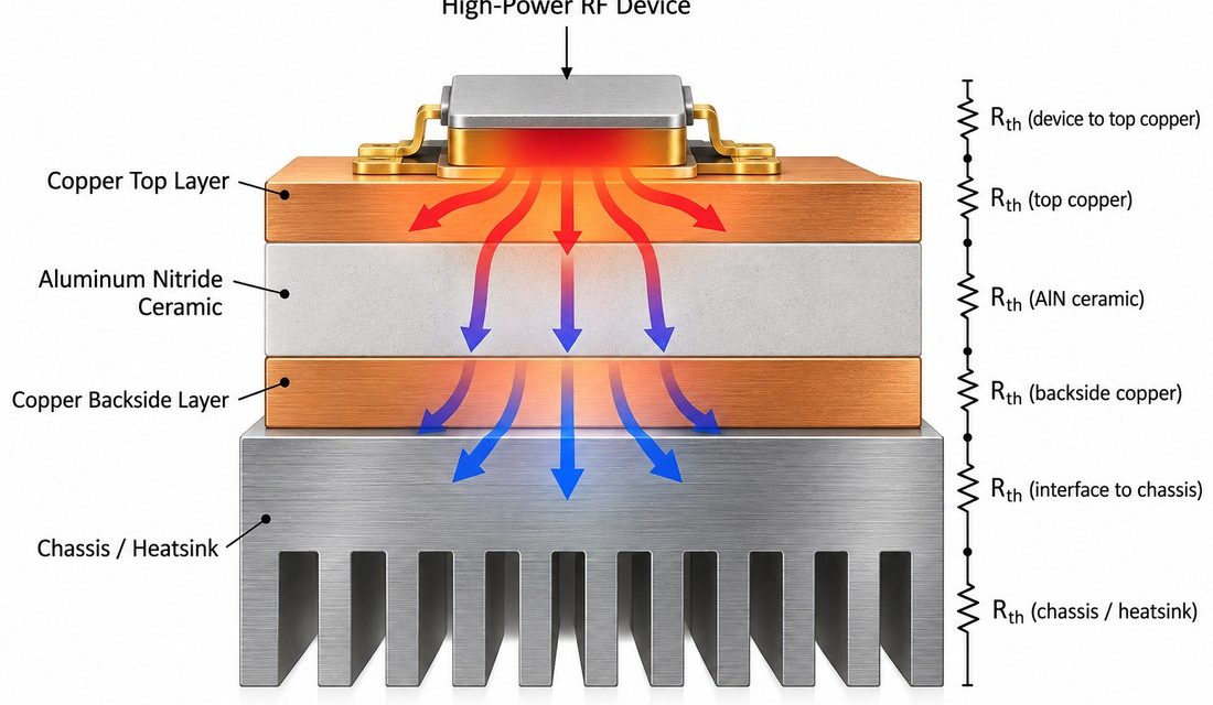
A power amplifier module can have a favorable ceramic thermal value and still miss its temperature margin because the heat path is not released as a complete assembly. An Aluminum Nitride PCB shares heat and RF functions with copper, solder or braze, a carrier, and the enclosure. The project pain is usually an interface assumption:...
Alumina PCB DFM: Metallization, Panel Handling, and Inspection Before Volume Release

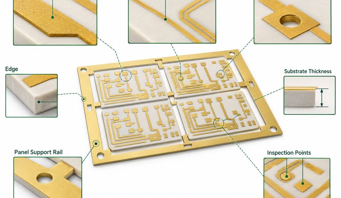
Volume release exposes the difference between a ceramic layout and a ceramic process. Screen, thick-film, thin-film, plated, brazed, and bonded features each have a different capability window. An Alumina PCB drawing that specifies only line widths and hole sizes can still leave the supplier guessing about paste, firing, edge handling, carrier support, and inspection. The...

PTFE PCB Loss Budgets: Copper Profile Checks for Long RF Paths

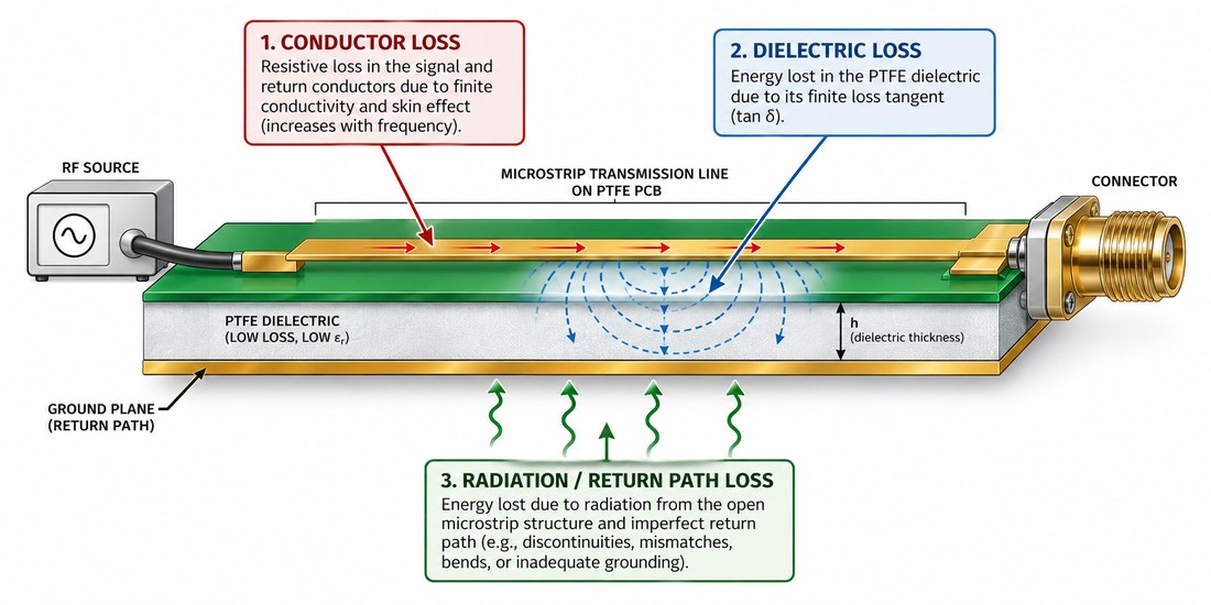
When a microwave path becomes long enough, the material name alone cannot explain insertion loss. A PTFE PCB combines dielectric loss, conductor roughness, trace geometry, resin or ceramic loading, connector transitions, and the return path. Engineers often discover the real problem during a system margin review because the original estimate used a catalog loss tangent...

Ceramic PCB Metallization and Via Reliability: A Practical Review for RF Power Boards

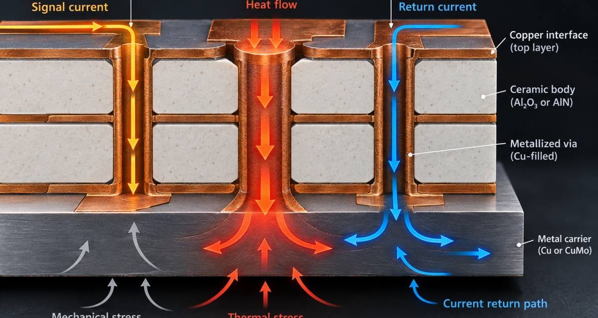
A ceramic substrate can be electrically stable and thermally efficient while the interconnect still becomes the weak point. Metallization adhesion, plated or filled vias, copper thickness, and the transition to a connector or carrier all experience different mechanical strain. For a Ceramic PCB used in a power or microwave module, the correct question is not...

Ceramic PCB Thermal Interfaces for High-Power RF Modules: A Release Review

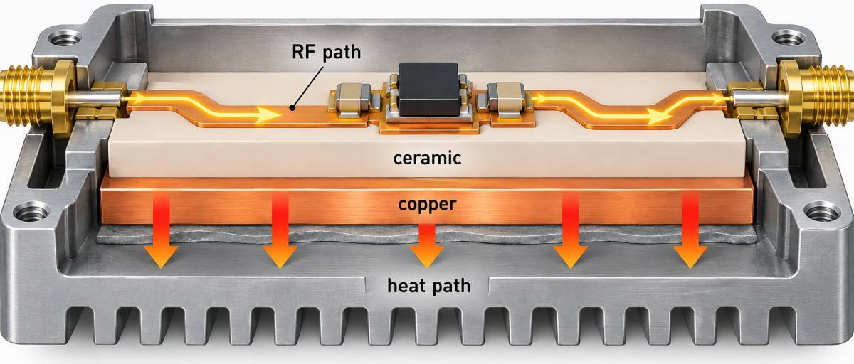
A high-power RF module can meet its electrical target and still fail in the field because the heat path was never released as a complete system. A Ceramic PCB changes the design conversation: the ceramic substrate, copper pattern, attach method, via or metallized interface, and the enclosure all share the same thermal boundary. The project...

Megtron 6 PCB Assembly: A Reflow and Connector-Launch Plan for High-Speed Modules

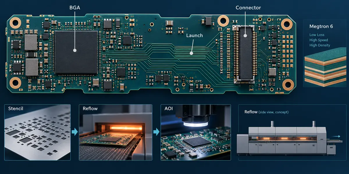
The Megtron 6 PCB connector launch remains the shared datum for SI and assembly inspection. The production Megtron 6 PCB callout should travel with the reflow and inspection package. A connector change on a Megtron 6 PCB is an electrical and assembly change, not only a mechanical edit. For the release team, a Megtron 6...

Taconic RF-35 PCB Drill and Plating Control: Avoiding PTFE Via Reliability Escapes

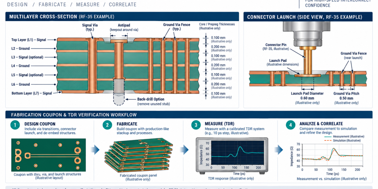
Table of Contents PTFE drilling and stackup RF drill table and transition geometry Desmear and plating controls Coupons and assembly handoff A via can pass an electrical design review and still become the first reliability escape in a PTFE-based RF build. Drill wander on a Taconic RF-35 PCB, smear removal, rough hole walls, poor copper...

Taconic RF-35 PCB Power Amplifier Layout: A Robust Heat-Spreading Path That Protects RF Tuning

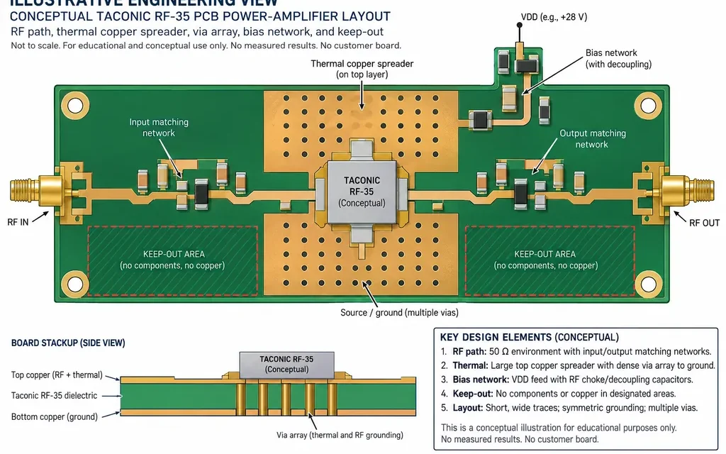
Taconic RF-35 PCB power amplifier thermal work must preserve two things at once: the device must shed heat, and the RF path must keep its intended impedance and return current. The common project failure is a late copper pour or thermal-via change that improves a temperature estimate but shifts the launch, bias isolation, or local...

TLY-5 PCB in Phased-Array Beamformers: A Thermal and Bias-Routing Strategy

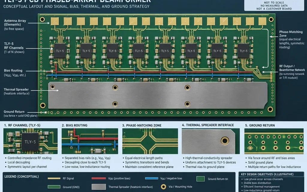
TLY-5 PCB beamformer thermal design is a coupled RF and power problem. In a phased array, each channel must preserve phase while bias networks, power amplifiers, control lines, and heat paths share a compact multilayer board. The engineering risk is not simply a hot spot; it is a hot spot that changes dielectric geometry, connector...

TLY-5 PCB Via Fields: Designing Plated Transitions Without Tuning Away the Real Problem

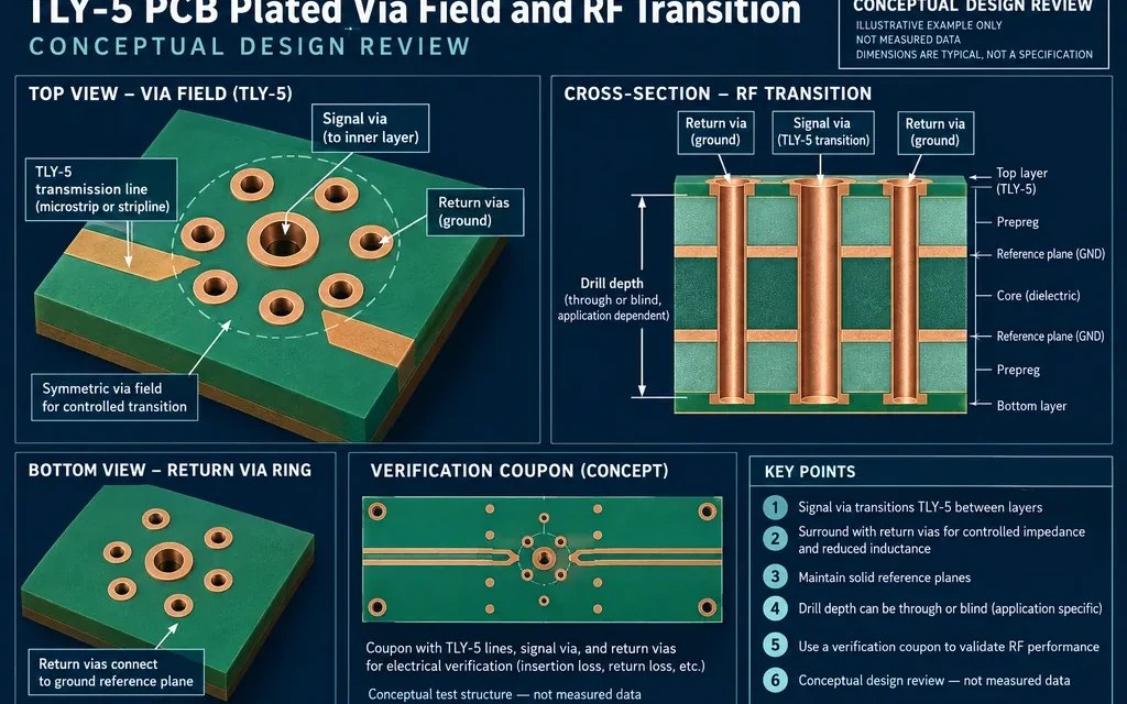
A TLY-5 PCB via field is not a cosmetic layout detail in a Ku-band module. The plated transition decides where the return current closes, how much barrel remains beyond the active layer, and whether the connector launch modeled by the RF team still represents the finished board. When this is released late, the first prototype...