
Taconic RF-35 PCB power amplifier thermal work must preserve two things at once: the device must shed heat, and the RF path must keep its intended impedance and return current. The common project failure is a late copper pour or thermal-via change that improves a temperature estimate but shifts the launch, bias isolation, or local dielectric environment.
Table of Contents
Build a device-level heat budget
List dissipation, duty cycle, case temperature, copper-plane area, thermal-via resistance, and enclosure contact. A calculated 2 W class envelope may be useful for planning, but it remains a target until the device and operating profile are fixed. Taconic RF-35 PCB placement should keep thermal escape away from the most sensitive launch datum. The RF PCB design design package should identify both the thermal path and the RF return path.
Keep bias and RF returns intentionally separate
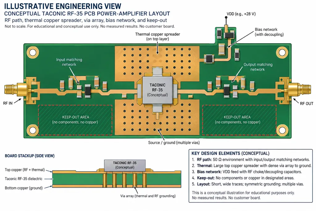
Bias decoupling needs short current loops while the RF path needs a continuous reference. Use layer assignments, via fences, and clearance rules that prevent a switching edge from crossing a phase-critical route. Taconic RF-35 PCB geometry should be reviewed after bias pours are complete. The PCB manufacturing high-frequency PCB check can record rail width, via sharing, capacitor placement, and the plane continuity that the model assumed.
Spread heat without creating a hidden capacitor
Large copper islands, exposed pads, and thermal vias alter local capacitance and current distribution. Model the device pad, ground vias, and nearby RF trace together. Taconic RF-35 PCB material assumptions should include finished copper and dielectric targets. The RF PCB materials RF PCB materials record should prevent an undocumented foil or finish change from being blamed on the thermal modification.
Make assembly part of thermal correlation
Exposed-pad solder volume, void limits, placement, and reflow history can move thermal resistance between channels. Use X-ray or an agreed inspection method for the thermal pad and protect connectors from rework. Taconic RF-35 PCB notes should call out the active device and launch relationship. The controlled-impedance PCB assembly handoff should separate bare-board acceptance from device-joint acceptance.
Release a combined RF and thermal gate
Freeze thermal targets, copper balance, via class, stackup, bias map, phase reference, and inspection evidence. Taconic RF-35 PCB documentation should distinguish a calculated junction estimate from a measured temperature. The PCB assembly manufacturing release then has a clear decision path if gain, temperature, or phase moves on the next build.
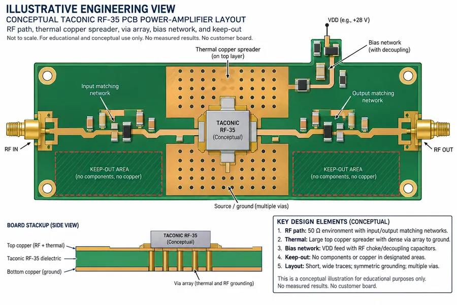
Treat heat spreading as part of the RF stackup review. A controlled copper plan, representative coupon, and assembly inspection record let the team improve power handling without losing the phase and gain repeatability the original layout was built to achieve.
Project evidence and handoff for Taconic RF-35 PCB power amplifier thermal
For a power-amplifier board, connect the thermal estimate to bias current, duty cycle, copper area, via field, enclosure contact, and RF return continuity. A temperature target without those assumptions is not enough to authorize a layout change. The Taconic RF-35 PCB drawing should make the critical datum visible to layout, fabrication, assembly, and test. If a number is calculated, retain the assumptions; if it is a supplier typical, keep it labeled as typical; if it is a measured acceptance value, keep the sample, method, and revision traceable.
| Release item | Engineering question | Evidence to retain |
|---|---|---|
| Stackup and material | Does the finished construction match the RF model? | Finished dielectric target, copper assumption, material lot, cross-section |
| Transition or critical path | Is the mechanical datum also the electrical datum? | Launch drawing, via or pad dimensions, mask and connector inspection |
| Process witness | Does the coupon represent the product feature? | Panel position, layer pair, finish, drill and impedance record |
| Assembly and test | Could placement, rework, or calibration move the result? | Placement tolerance, reflow or rework history, fixture and reference plane |
For program control, use a short disposition statement after each build: what passed, what moved, what is still a target, and which owner decides the next change. This keeps the Taconic RF-35 PCB power amplifier thermal discussion focused on evidence and prevents a new material, finish, or layout change from being introduced without an updated model and acceptance plan.
Sources: Taconic and Rogers typical material data; IPC-TM-650 methods relevant to dielectric, copper, drilling, plating, registration, and impedance; RF application guidance from Qorvo, Analog Devices, and Würth Elektronik; KKPCB PCB design, materials, manufacturing, assembly, and high-frequency capability pages. Values are typical, target, or calculated references unless explicitly identified as measured.
