
When a microwave path becomes long enough, the material name alone cannot explain insertion loss. A PTFE PCB combines dielectric loss, conductor roughness, trace geometry, resin or ceramic loading, connector transitions, and the return path. Engineers often discover the real problem during a system margin review because the original estimate used a catalog loss tangent but not the actual copper profile or fabricated width. A PTFE PCB loss budget should also include the fabricated copper profile and connector transition, not only the laminate data sheet. This PTFE PCB review keeps the design target separate from any measured production coupon.
Build the budget from the signal path
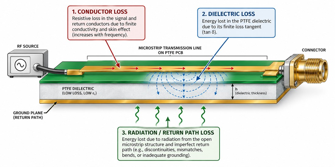
Divide the channel into launch, transmission line, bend or taper, via transition, connector, and receiver entry. Assign each section a design target and note whether the number is from a supplier typical value, a field-solver estimate, or a measured coupon. A PTFE PCB is most effective when the budget identifies which section can consume the remaining margin.
Dielectric loss and conductor loss respond differently to frequency, length, and copper texture. A smooth copper option may reduce conductor loss, but it can also change adhesion or process cost. The RF PCB material review should record the copper treatment, foil type, and etch compensation assumptions instead of listing only the laminate family.
Use the finished geometry, not just the artwork width, in the calculation. Plating, resin squeeze, solder mask, and weave or filler distribution can move the impedance. A reasonable engineering range is more useful than a false decimal precision when the supplier has not yet released the stack.
Keep geometry and return path stable
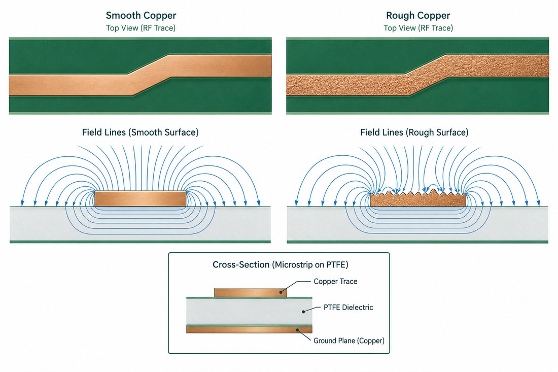
A low-loss line still needs a low-inductance return path. Keep the reference plane continuous, control the spacing to the plane, and avoid abrupt neck-downs at test pads or component lands. Analog Devices RF layout guidance recommends preserving the return path and using nearby ground features when a signal changes layers; apply the same discipline to the PTFE PCB launch and via field.
If the design uses a coplanar waveguide, set the ground clearance from the actual stackup and surface finish. The controlled impedance layout file should identify where the ground pour is intentional and where it is a keep-out. Do not allow an automatic CAD pour to decide the coupling gap.
At the review gate, compare nominal, minimum, and maximum finished geometry. Release the acceptable impedance window and the reference coupon geometry together so the fabricator can tune the process without changing the RF intent.
Make the loss budget useful to the project manager
The project plan should show which materials or copper options are long-lead, which dimensions need a coupon, and which margin is reserved for connector variation. A thermal management production note that says “low loss” is not enough for a high-frequency channel; it must state the frequency range, line type, and acceptance method.
When a supplier suggests an alternate PTFE construction, review Dk, loss, copper, thickness, and process compatibility as a set. A near-equivalent dielectric value does not prove equivalent insertion loss if the copper treatment or finished thickness changes.
Close the design with a short table: path length, target loss, geometry, material assumption, coupon, and owner. That turns a material decision into a procurement and validation plan.
A PTFE PCB loss budget is a living engineering model. Tie dielectric data to finished geometry, copper profile, return path, and coupon evidence so the project can trade cost and margin without guessing.
Implementation note for this low-loss line and copper profile review: keep the engineering assumption visible at the point where it affects a drawing, a supplier quote, or an inspection record. Ask the design owner to identify the reference plane, interface datum, and acceptance method before the release is frozen. Ask manufacturing to return the proposed stack, panel, and process window rather than a generic capability statement. Ask assembly to identify the profile, cleaning, and support conditions that could move the RF or thermal result. This simple handoff prevents a typical material value from being mistaken for a guaranteed product result and gives the project team a clear action when an ECO changes the physical boundary.
undefined
Sources: Panasonic MEGTRON technical material guidance; Rogers and Taconic high-frequency material data sheets where relevant; CeramTec ceramic substrate data; Analog Devices RF and mixed-signal layout guidance. Numerical values are treated as typical supplier values or engineering targets unless the released drawing defines a measured acceptance value.
Release note: confirm the PTFE PCB construction before the next ECO.
Release note: confirm the PTFE PCB construction before the next ECO.
Release note: confirm the PCB manufacturing evidence before approval.
Release note: confirm the PCB assembly evidence before approval.
For project handoff, keep the PTFE PCB loss budget tied to the released stack-up, copper profile, and line geometry so procurement cannot substitute a lower-loss material with an uncontrolled surface finish.
