
TLY-5 PCB beamformer thermal design is a coupled RF and power problem. In a phased array, each channel must preserve phase while bias networks, power amplifiers, control lines, and heat paths share a compact multilayer board. The engineering risk is not simply a hot spot; it is a hot spot that changes dielectric geometry, connector position, or bias noise while the array is being calibrated.
Table of Contents
Map the beamformer heat path before routing RF channels
Start with the amplifier dissipation estimate, duty cycle, copper-plane area, thermal-via field, and enclosure contact. A calculated 1.5–2.5 W per active channel can be a useful design envelope, but it is a target until the actual device and duty cycle are confirmed. TLY-5 PCB channel placement should keep the hottest devices away from connector datums and the most phase-sensitive launches. The RF PCB design review should show where heat leaves the board and where it could distort the RF reference plane.
Separate bias-current geometry from phase-critical return paths
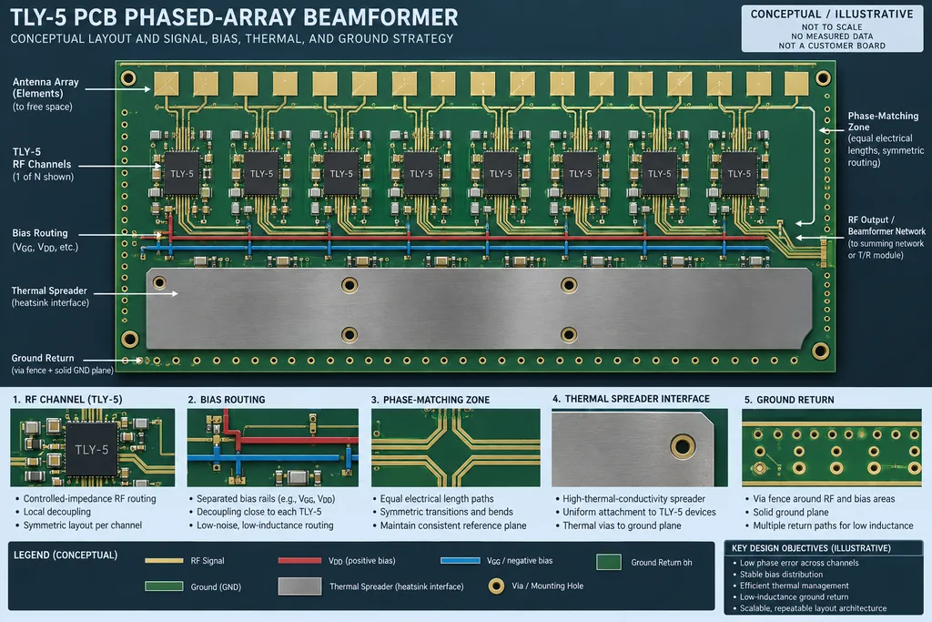
Bias rails need low impedance and controlled decoupling, but their copper should not casually interrupt an RF return plane. Use a layer plan that gives the RF path a continuous reference, then bring bias vias through defined clearances. TLY-5 PCB trace geometry should be checked after bias pours, not before. The PCB manufacturing stackup review can record rail width, via sharing, decoupling location, and the clearance that prevents a switching edge from entering a sensitive channel.
Use copper spreading without creating an RF discontinuity
A solid copper spreader helps temperature, yet a large copper island can change local capacitance and effective dielectric environment. Model the region around the amplifier, transition, and heat-via array together. Keep the TLY-5 construction and finished copper assumption visible. TLY-5 PCB thermal copper must be balanced with the launch geometry; RF PCB materials material and finish choices should remain tied to the same revision so a thermal improvement does not become an undocumented RF change.
Define assembly controls for the active array
The placement program should control amplifier rotation, pad registration, exposed-pad solder volume, void limits, and connector coplanarity. A board can pass bare-board inspection while an uneven exposed-pad joint changes thermal impedance between channels. Use TLY-5 PCB drawings to identify phase-critical connectors and use controlled-impedance PCB inspection and rework rules to protect them. Record which values are targets, which are supplier typicals, and which are measured on the released build.
Release a channel-level correlation plan
Correlate one representative channel before scaling the array. The plan should define temperature condition, bias state, calibration plane, phase window, and the coupon or witness structure. TLY-5 PCB documentation should link the channel stackup to the measured reference plane. After the RF check, the PCB assembly manufacturing handoff can freeze panel location, copper balance, thermal-via drill class, and assembly revision for the next build.
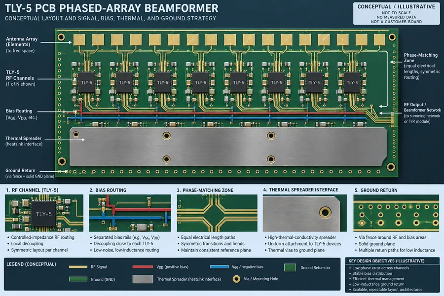
A release package should therefore connect beamformer phase budgets, bias-current maps, thermal spreading assumptions, stackup targets, and assembly inspection. Treat the TLY-5 PCB as the mechanical, RF, and thermal reference for the whole channel rather than as a passive laminate selection.
Project evidence and handoff for TLY-5 PCB beamformer thermal
For a phased-array board, the useful project record is a channel-level map: device dissipation, bias state, copper spreader, thermal-via field, RF reference plane, connector datum, and phase allocation. The team should note which channel was used for correlation and which values are still design targets. The TLY-5 PCB drawing should make the critical datum visible to layout, fabrication, assembly, and test. If a number is calculated, retain the assumptions; if it is a supplier typical, keep it labeled as typical; if it is a measured acceptance value, keep the sample, method, and revision traceable.
| Release item | Engineering question | Evidence to retain |
|---|---|---|
| Stackup and material | Does the finished construction match the RF model? | Finished dielectric target, copper assumption, material lot, cross-section |
| Transition or critical path | Is the mechanical datum also the electrical datum? | Launch drawing, via or pad dimensions, mask and connector inspection |
| Process witness | Does the coupon represent the product feature? | Panel position, layer pair, finish, drill and impedance record |
| Assembly and test | Could placement, rework, or calibration move the result? | Placement tolerance, reflow or rework history, fixture and reference plane |
For program control, use a short disposition statement after each build: what passed, what moved, what is still a target, and which owner decides the next change. This keeps the TLY-5 PCB beamformer thermal discussion focused on evidence and prevents a new material, finish, or layout change from being introduced without an updated model and acceptance plan.
Sources: Taconic and Rogers typical material data; IPC-TM-650 methods relevant to dielectric, copper, drilling, plating, registration, and impedance; RF application guidance from Qorvo, Analog Devices, and Würth Elektronik; KKPCB PCB design, materials, manufacturing, assembly, and high-frequency capability pages. Values are typical, target, or calculated references unless explicitly identified as measured.
