HomeTag

DFM - KKPCB

How to Release an IoT Sensor PCB for Repeatable Volume Calibration

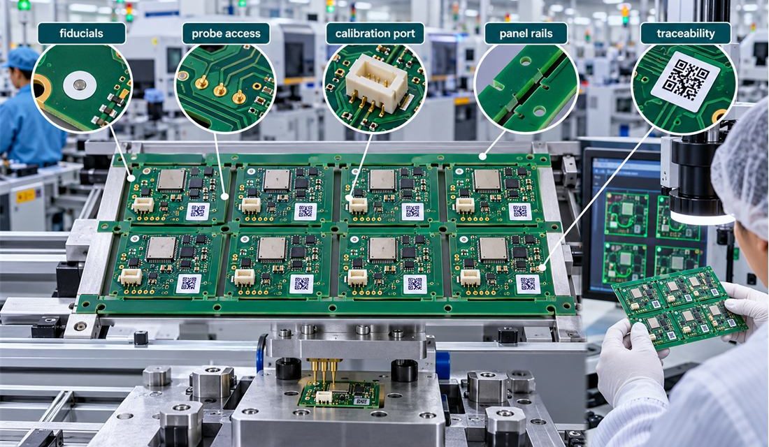
Table of Contents Why a stable design still fails at volume Design the panel for inspection Make calibration repeatable Control revision and supplier changes A prototype can produce excellent sensor readings and still become a difficult product to build. The problems appear when a small IoT Sensor PCB moves into panels, fixtures, alternate components, and...
Aluminum Nitride PCB Inverter Modules: DFM, Panel Handling, and Production Release Controls

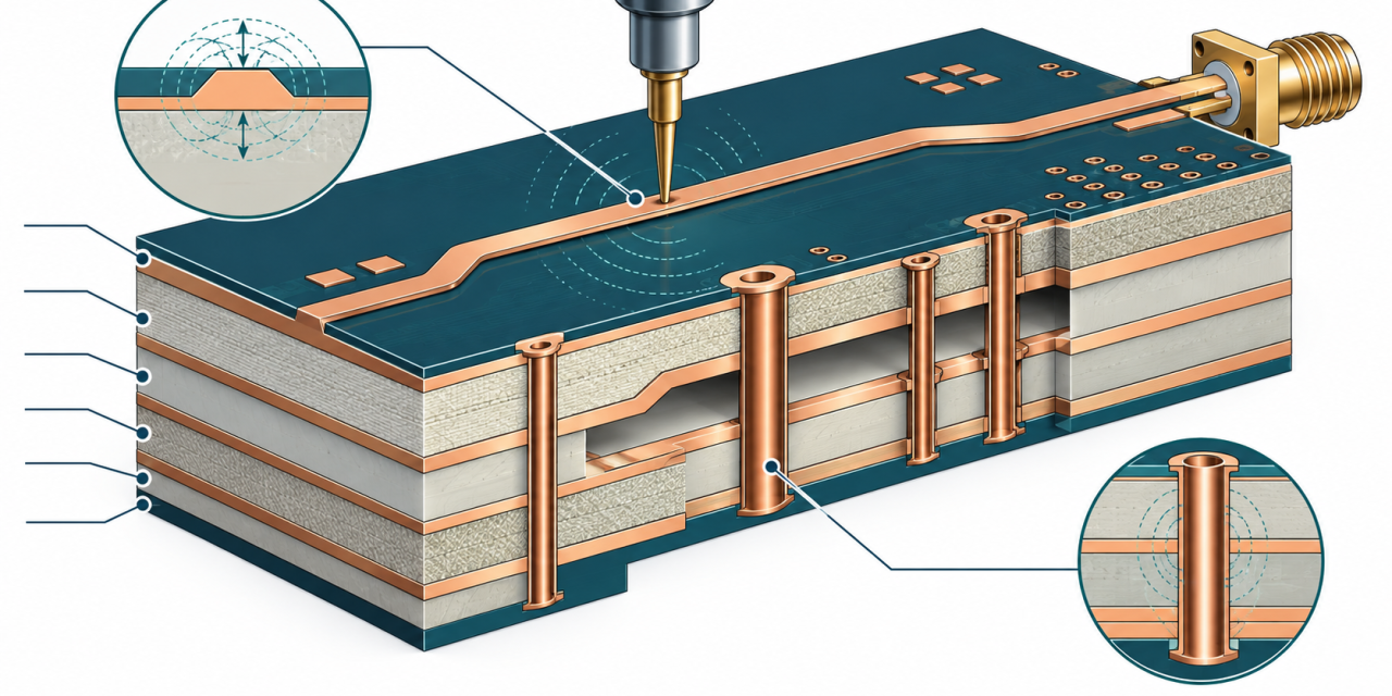
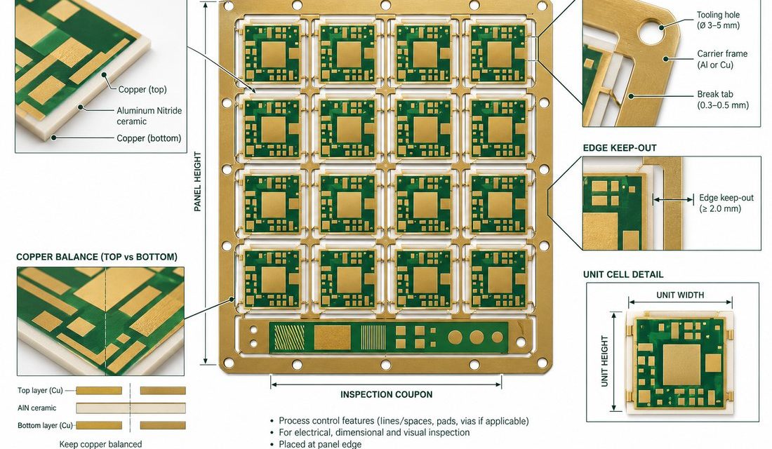
An Aluminum Nitride PCB inverter module release should connect panel handling, copper interfaces, and inspection evidence before production volume is authorized. Inverter modules expose the difference between a ceramic concept and a repeatable production process. Heavy copper, AlN substrate, switching devices, isolation clearances, carrier support, and inspection access all compete for the same panel area....

Alumina PCB DFM: Metallization, Panel Handling, and Inspection Before Volume Release

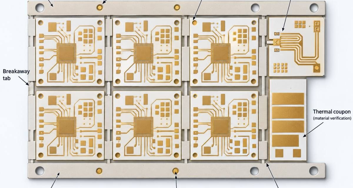
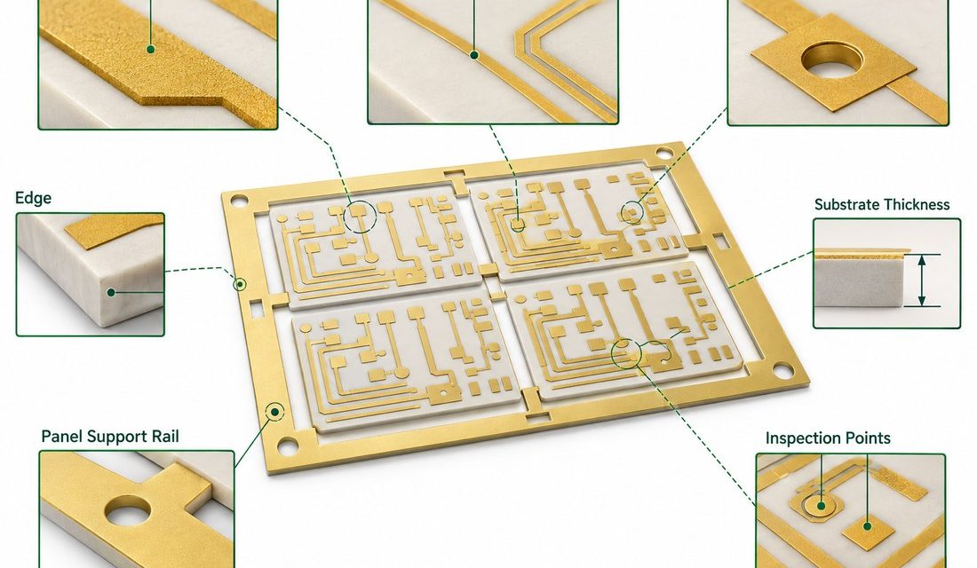
Volume release exposes the difference between a ceramic layout and a ceramic process. Screen, thick-film, thin-film, plated, brazed, and bonded features each have a different capability window. An Alumina PCB drawing that specifies only line widths and hole sizes can still leave the supplier guessing about paste, firing, edge handling, carrier support, and inspection. The...

PTFE PCB DFM: Panelization and Procurement Controls for Repeatable RF Builds

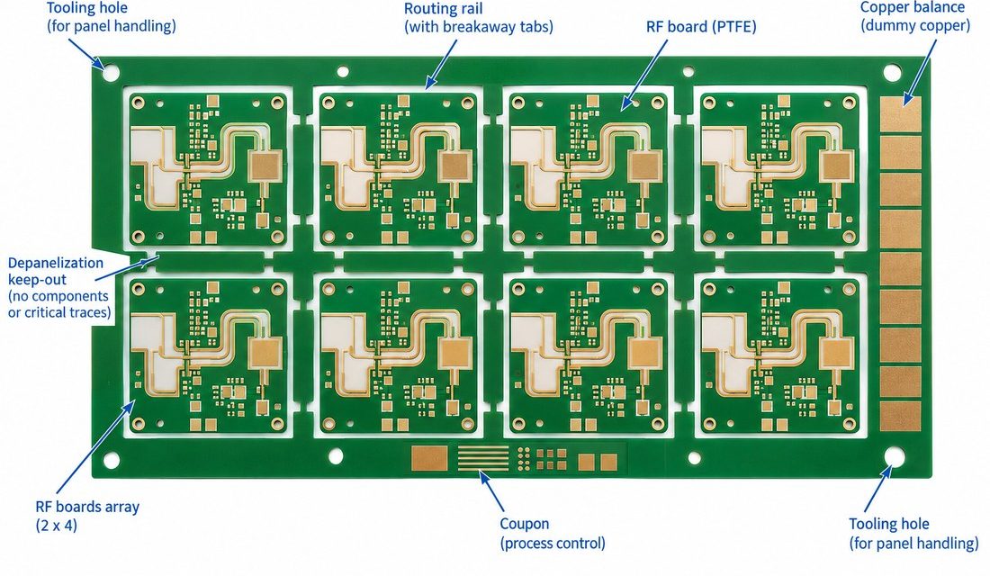
A PTFE board can be electrically well designed and still be difficult to quote or panelize. The manufacturing risk is concentrated at the interfaces: copper balance, drilled features, plated edges, hybrid stackup boundaries, connector rails, and the coupon that is supposed to represent the RF path. A PTFE PCB release should therefore explain the process...

Ceramic PCB DFM and Procurement Release: Avoiding First-Build Surprises

Ceramic PCB programs often move from concept to purchase order faster than the manufacturing package matures. The layout may be complete, but the supplier still lacks a defined panel, edge condition, metallization note, inspection plan, or approved substitute rule. That gap creates schedule risk because a ceramic panel is not interchangeable with a conventional laminate...

Rigid Flex PCB Cost Optimization

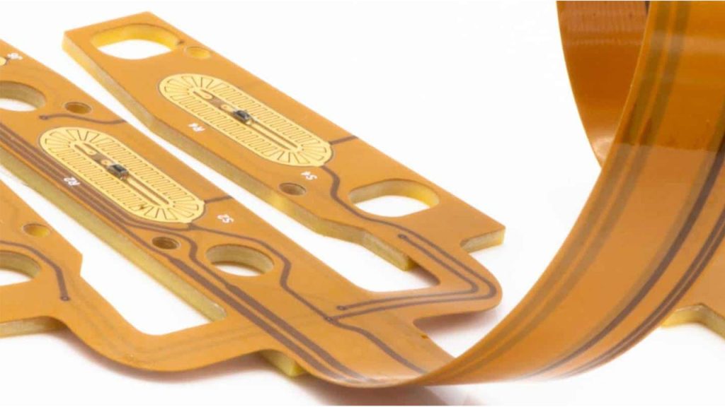
Master Your Budget: Proven Strategies for Rigid Flex PCB Cost Optimization In modern electronics, Rigid-Flex PCB technology is the gold standard for compact, high-reliability designs. However, the complexity of Rigid-Flex manufacturing often leads to higher production expenses. Achieving effective Rigid Flex PCB cost optimization requires a strategic balance between sophisticated engineering and smart logistical choices. At KKPCB, we help engineers navigate these...

The Five Golden Rules of PCB Design

Printed Circuit Board (PCB) design is a critical step in the development of any electronic product. A well-designed PCB ensures reliability, performance, and manufacturability, while a poor design can lead to costly failures and delays. Below are five golden rules that every PCB designer should follow. 1. Prioritize Clear and Logical Layout A clean and...