
RO4350B PCB impedance drift is the manufacturing risk this release checklist is designed to control.
When a multilayer RF project moves from layout to fabrication, the most expensive surprise is often not a missing feature but a changed impedance. An RO4350B PCB can meet the designer’s target only when the stackup, copper definition, laminate lot, etch compensation, and measurement method are handed off as one controlled system. This guide uses an illustrative manufacturing handoff to show how to prevent impedance drift without claiming a KKPCB customer result.
Why impedance changes after the design is frozen
Engineers frequently freeze a 50 ohm trace in the CAD tool and send only width and spacing to the fabricator. The fabricator still has to interpret finished dielectric thickness, copper treatment, foil profile, resin fill, and the reference-plane geometry. Each interpretation changes the field distribution around the trace.
Rogers lists RO4350B process Dk as a typical 3.48 ± 0.05 and a design Dk of 3.66; the datasheet also lists a typical Df of 0.0037 and thermal conductivity of 0.69 W/m·K. These are vendor-typical material values, not a guaranteed value for every finished board. The stackup calculator should therefore use the supplier’s controlled construction and the finished dimensions that will be checked in production.
| Handoff item | Typical failure mode | Preventive control |
|---|---|---|
| Dielectric thickness | Finished spacing differs from the nominal core or prepreg callout. | Specify finished dielectric targets and an approved tolerance window. |
| Copper profile and etch | Trace width changes at the sidewall, shifting calculated impedance. | Provide finished copper, profile class, and etch-compensation rules. |
| Reference plane | Voids, antipads, or split planes alter local return current. | Review planes in the same cross-section used for the impedance coupon. |
| Test method | TDR result is compared with a different coupon geometry. | Lock coupon layer, line style, launch, and acceptance method before release. |
Build a stackup that the factory can reproduce
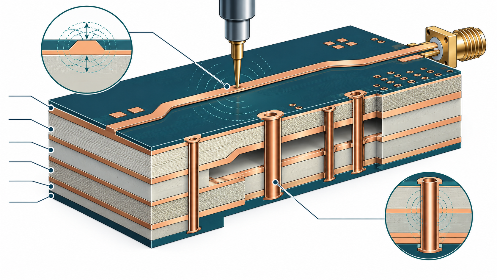
Start with the electrical goal, then translate it into a manufacturable cross-section. For an RF module, place the critical microstrip or stripline next to a continuous reference plane, keep its dielectric spacing explicit, and reserve a separate routing layer for power and low-speed nets. A compact RO4350B PCB stackup can be combined with FR-4 cores away from the RF path, but the material transition must be shown in the drawing and reviewed for resin flow and registration.
In an illustrative eight-layer handoff, the RF layer may use RO4350B with a controlled finished dielectric, inner reference planes may be solid copper, and the outer digital layers may use a compatible construction. The numbers are design targets only; the final press cycle, copper weights, and panel orientation must be confirmed in DFM. If the project needs HDI escape routing, link the RF layer plan to an HDI PCB review rather than adding microvias after the stackup has been quoted.
Use one dielectric definition everywhere
CAD, fabrication drawing, impedance table, and coupon drawing must use the same definition: core or prepreg thickness, finished copper, and whether the value is before or after press. A reliable RO4350B PCB handoff records the material family, nominal thickness, copper foil type, and the approved alternative construction. If a supplier proposes a different press combination, the change should trigger a fresh impedance calculation rather than a verbal approval.
Control routing and transitions before the DFM review
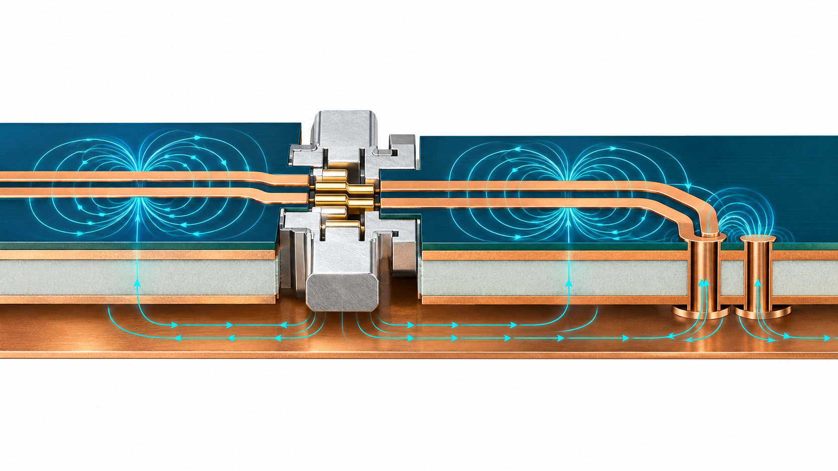
Impedance is not only a straight-line problem. Connector launches, pad neck-downs, via antipads, and layer transitions can dominate return loss even when the long trace is correct. Keep the reference plane unbroken under the launch, use a short neck-down, and place ground stitching vias close enough to preserve the return path. The second generated figure illustrates this return-current idea.
Set practical drawing and inspection gates
- Freeze the controlled-impedance table with layer, line style, target, tolerance, and test coupon reference.
- Mark every RF transition and identify the reference plane on the fabrication drawing.
- Ask for the proposed stackup and impedance field solver result during DFM, before tooling.
- Approve the coupon location and launch geometry; do not accept a generic coupon by default.
- Record any construction substitution and rerun the calculation before release.
Illustrative project decision: prototype to production
Consider a compact RF control board that passes bench bring-up but shows inconsistent return loss between prototype panels. The likely project pain is not the RO4350B material itself; it is an uncontrolled construction change. The project manager can reduce risk by requiring a single approved stackup, a controlled coupon, and a first-article report that separates calculated target, vendor-typical material data, and measured production values.
For production, a PCB manufacturing partner should confirm panel orientation, copper distribution, registration plan, and the DFM response in writing. KKPCB’s public manufacturing pages describe multilayer, high-frequency, HDI, mixed-material, sequential-lamination, and controlled-impedance capabilities; the exact construction remains quote-specific. A project team can also use the multilayer PCB service page to align layer count and press constraints before releasing Gerbers.
Checklist for a stable RO4350B PCB release
- Exact RO4350B laminate and thickness are named, with a permitted substitute process.
- Finished dielectric and copper targets are stated, not only nominal laminate codes.
- RF traces, reference planes, antipads, and stitching vias are reviewed as one field structure.
- Coupon geometry matches the controlled layer and line style.
- Every numeric value is labeled as vendor-typical, design target, calculated estimate, or measured result.
- Prototype-to-production changes require a new stackup and impedance review.
Sources: Rogers RO4350B product-properties and laminate data are used as vendor-typical reference values; KKPCB public PCB materials, high-frequency PCB, HDI PCB, multilayer PCB, and PCB manufacturing pages are used to verify available service categories. This article contains no external hyperlinks and does not claim a KKPCB customer measurement.
RO4350B PCB release controls for procurement
A repeatable RO4350B PCB build starts with a signed construction table. The table should identify the RO4350B PCB layer, finished dielectric, copper profile, and coupon. A second RO4350B PCB review should confirm that the multilayer press plan still matches the impedance model.
When a supplier proposes a substitute, compare it against the released RO4350B PCB stackup rather than approving a material name by email. The RO4350B PCB drawing should show RF transitions, plane openings, and inspection points. This keeps the RO4350B PCB design intent visible to purchasing, DFM, and quality teams.
- Use one RO4350B PCB stackup file for CAD, quotation, and inspection.
- Record the RO4350B PCB coupon and acceptance method in the purchase package.
- Recalculate any RO4350B PCB substitution before production release.
RO4350B PCB impedance drift acceptance gate
Use the RO4350B PCB impedance drift phrase as a release gate: compare the approved stackup, finished dimensions, coupon geometry, and first-article evidence before production.
- Log each RO4350B PCB impedance drift review as a controlled engineering change.
- Keep the RO4350B PCB impedance drift acceptance method with the purchase package.
