HomeCategory

PCB Materials | FR-4, High-Frequency, Low-Loss & Heavy Copper - KKPCB

The Significance of Impedance in PCB Design and Manufacturing

With the continuous development of high-speed electronics, modern PCB designs are becoming increasingly complex. Higher data rates, faster signal transitions, and more compact product structures have made signal integrity a critical factor in electronic system performance. In traditional low-speed PCB applications, traces are mainly considered simple electrical connections. However, when signal frequencies increase, PCB traces...
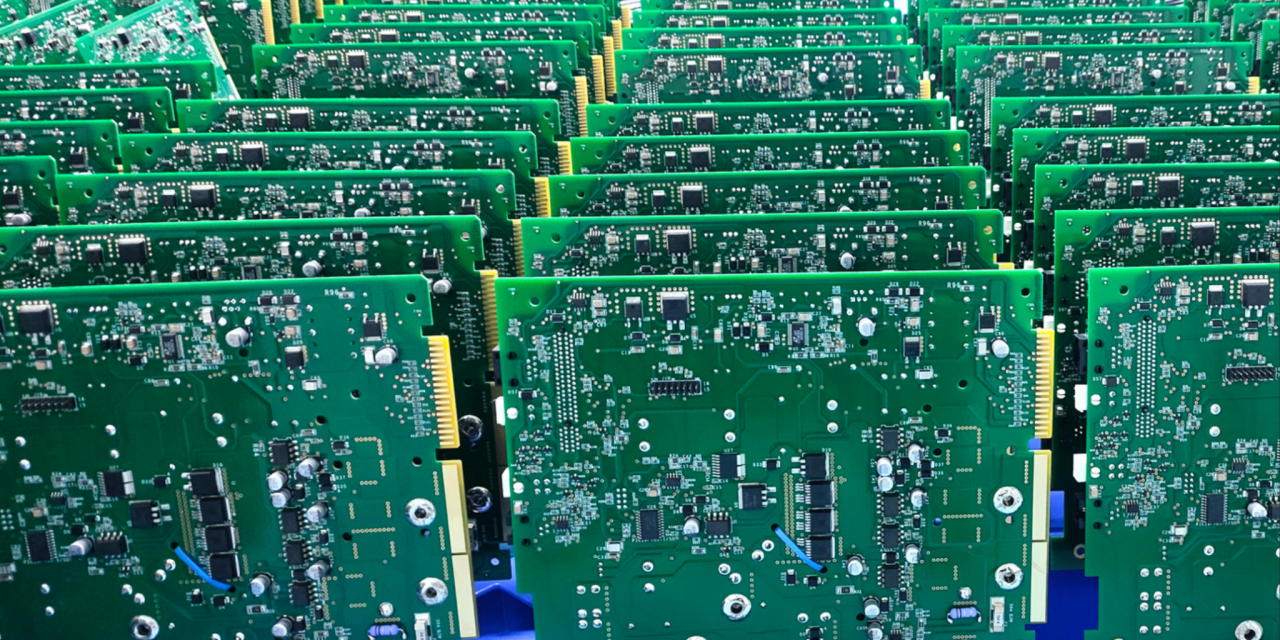
Detailed Explanation of PCB Manufacturing Process and Precautions

Printed Circuit Board (PCB) manufacturing is a complex process that transforms a circuit design into a physical electronic platform capable of supporting components and enabling reliable electrical connections. As the foundation of almost all electronic products, PCB quality directly influences: Electrical performance Product reliability Assembly efficiency Long-term operating stability From consumer electronics and industrial control...

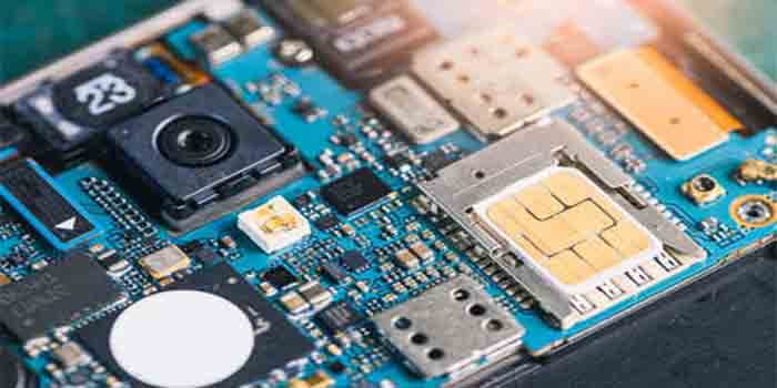
Mobile Phone PCB Layout: Key Considerations and Wiring Best Practices

Engineering Context Modern smartphones integrate increasingly complex electronic functions into extremely compact form factors. A mobile phone PCB must support high-speed processors, 5G communication modules, RF front-end circuits, camera systems, power management units, sensors, wireless charging, and high-density memory devices while maintaining reliability and signal performance. Unlike traditional electronic boards, Mobile Phone PCB design requires...

Basic Rules for PCB Layout and Wiring

Printed Circuit Board (PCB) layout and wiring are essential processes that transform a circuit schematic into a manufacturable electronic product. A well-designed PCB not only ensures electrical performance but also improves reliability, thermal management, production efficiency, and long-term stability. As electronic products become smaller and more powerful, PCB designs face increasing challenges such as higher...

PCB Plating Hole Filling Technology

As electronic products continue to evolve toward higher density, faster signal transmission, and greater reliability, traditional through-hole processing is no longer sufficient for many advanced PCB designs. Technologies such as HDI (High-Density Interconnect), BGA (Ball Grid Array), and fine-pitch surface-mount devices often require plated through holes with improved mechanical strength and completely sealed surfaces. PCB...

Application of waterproof material on pcb and FPC proofing

With the rapid development of electronic products toward miniaturization, lightweight design, and higher reliability, PCB and FPC technologies are increasingly applied in environments where exposure to moisture, humidity, water splash, chemicals, and dust cannot be avoided. Applications such as automotive electronics, wearable devices, medical equipment, industrial control systems, outdoor monitoring devices, and smart sensors require...

PCB Screen Printing Stencil Making Process

In modern PCB assembly, solder paste printing is one of the most critical steps in the SMT manufacturing process. Before components are placed and soldered, a precise amount of solder paste must be deposited onto specific PCB pads. The quality of this process directly affects: solder joint reliability, component placement accuracy, assembly yield, production consistency....

What is the Significance of Solder Paste Printing?

1. Introduction: Why Solder Paste Printing Is Critical in SMT Assembly In modern PCB assembly (PCBA) manufacturing, especially in Surface Mount Technology (SMT) processes, solder paste printing is one of the most critical initial steps. Although it may appear simple, solder paste printing directly determines the quality of: Component placement accuracy Solder joint strength Electrical...

Industrial PCB Production

Industrial PCB Production In today’s rapidly evolving industrial landscape, Printed Circuit Boards (PCBs) serve as the critical backbone of automation systems, control equipment, heavy machinery, robotics, and smart manufacturing solutions. Industrial PCB production demands far higher standards than consumer electronics. Boards must deliver exceptional reliability, durability under extreme conditions (vibration, temperature fluctuations, humidity, and dust),...

What is PCB warpage?

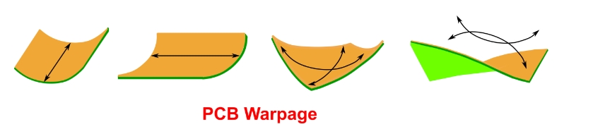
What is PCB Warpage? PCB warpage refers to the unwanted bending, twisting, or deformation of a printed circuit board from its intended flat shape. Ideally, a PCB should maintain a flat and stable surface throughout fabrication, assembly, and operation. However, differences in material properties, thermal expansion, copper distribution, and manufacturing processes can cause the PCB...