
Engineering Context
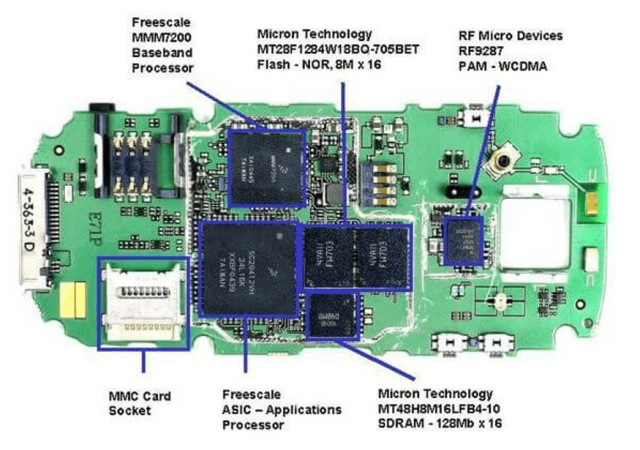
Modern smartphones integrate increasingly complex electronic functions into extremely compact form factors. A mobile phone PCB must support high-speed processors, 5G communication modules, RF front-end circuits, camera systems, power management units, sensors, wireless charging, and high-density memory devices while maintaining reliability and signal performance.
Unlike traditional electronic boards, Mobile Phone PCB design requires precise control of electrical, mechanical, thermal, and manufacturing factors. The continuous reduction in device thickness and the increasing number of components create significant challenges in PCB layout optimization.
A smartphone PCB typically includes:
- Application processors
- 5G RF transceiver circuits
- Power management ICs
- LPDDR memory
- Camera interface circuits
- Display interfaces
- Wi-Fi and Bluetooth modules
- Battery management systems
The PCB layout directly affects:
- Signal integrity
- Power integrity
- EMI performance
- Battery efficiency
- Thermal behavior
- Product reliability
Advanced mobile devices commonly use HDI PCB, microvia structures, fine-line routing, and high-layer-count multilayer PCB technologies to achieve compact designs while maintaining electrical performance.
For mobile phone manufacturers and procurement teams, selecting an experienced PCB supplier is essential. The supplier must understand not only PCB fabrication but also high-density routing, RF performance, material selection, and volume production consistency.
KKCPB provides advanced Mobile Phone PCB solutions, combining HDI manufacturing, RF PCB technology, impedance control, signal integrity analysis, and mass production capability for next-generation mobile communication products.
Core Engineering Challenges
| Engineering Challenge | Root Cause | Engineering Impact |
|---|---|---|
| Limited PCB space | Increasing component density | Difficult routing and layer management |
| High-speed signal degradation | Fast processors and memory interfaces | Data errors and performance loss |
| RF interference | Multiple wireless systems operating together | Reduced communication quality |
| Power integrity issues | High current processor loads | Voltage instability |
| Thermal concentration | Compact enclosure design | Component lifetime reduction |
| Manufacturing tolerance | Fine-pitch structures | Lower production yield |
These challenges make smartphone PCB layout one of the most demanding PCB engineering applications, requiring advanced HDI manufacturing and precise process control.
Mobile Phone PCB Layout Design Fundamentals
High-Density Routing Strategy
Modern smartphones use complex multilayer PCB structures to achieve compact layouts.
Key design approaches include:
- HDI microvia technology
- Laser drilling
- Fine-line trace routing
- Via-in-pad structures
- Sequential lamination
Typical HDI PCB structures include:
- 1+N+1 HDI
- 2+N+2 HDI
- Any-layer HDI
These structures allow engineers to place more components while reducing PCB size.
Signal Integrity Optimization
High-speed interfaces in smartphones require careful routing.
Common high-speed signals include:
- USB 3.x
- MIPI Display Interface
- MIPI Camera Interface
- LPDDR Memory
- PCIe Interface
Engineering practices include:
- Controlled impedance routing
- Differential pair matching
- Length tuning
- Reference plane optimization
- Crosstalk reduction
RF Layout Considerations
Smartphones contain multiple wireless systems:
- 5G communication
- Wi-Fi
- Bluetooth
- NFC
- GPS
RF PCB layout requires:
- 50Ω impedance control
- Antenna matching circuits
- RF isolation zones
- Ground shielding
- Low-loss materials
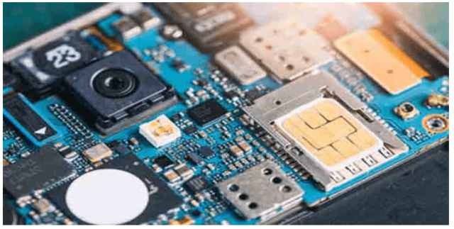
For advanced communication devices, materials such as RO4003C PCB, RO4350B PCB, and low-loss laminates may be used in RF sections to improve signal performance.
Material Science & PCB Performance Selection
Smartphone PCBs require materials balancing electrical performance, reliability, cost, and manufacturability.
Mobile Phone PCB Material Comparison
| Material | Application | Engineering Advantage |
|---|---|---|
| Standard FR-4 PCB | General circuits | Cost-effective solution |
| High TG PCB | Processor and power areas | Improved thermal reliability |
| HDI PCB Material | High-density routing | Supports microvia structures |
| RO4003C PCB | RF modules | Low-loss signal transmission |
| RO4350B PCB | Wireless communication | Stable dielectric performance |
| Low Dk Material | High-speed interfaces | Reduced signal delay |
Key Engineering Parameters
| Parameter | Importance |
|---|---|
| Dielectric Constant (Dk) | Controls signal propagation speed |
| Dissipation Factor (Df) | Influences signal loss |
| Copper Thickness | Affects current capacity |
| CTE | Determines dimensional stability |
| Tg | Controls thermal reliability |
| Surface Finish | Affects assembly quality |
KKCPB Case Study — 5G Smartphone Mainboard PCB Layout Optimization
Client & Application Context
A consumer electronics company developing a next-generation 5G smartphone required a high-density PCB solution.
The smartphone platform included:
- 5G RF transceiver
- Application processor
- LPDDR memory
- Multi-camera system
- Wi-Fi 6 module
- Wireless charging circuit
The customer required a compact PCB design with improved RF performance and stable mass production capability.
Engineering Problem
The initial PCB layout experienced several issues:
- High-speed signal interference
- Limited routing space
- RF coupling between antenna circuits and digital circuits
- Thermal hotspots near processor area
- Difficult manufacturing yield control
Engineering analysis showed:
- Memory signal skew exceeding specification
- EMI interference affecting RF sensitivity
- Local temperature increase around power ICs
- Microvia reliability concerns
The customer required a PCB manufacturing partner capable of optimizing layout and production processes.
KKCPB Engineering Solution
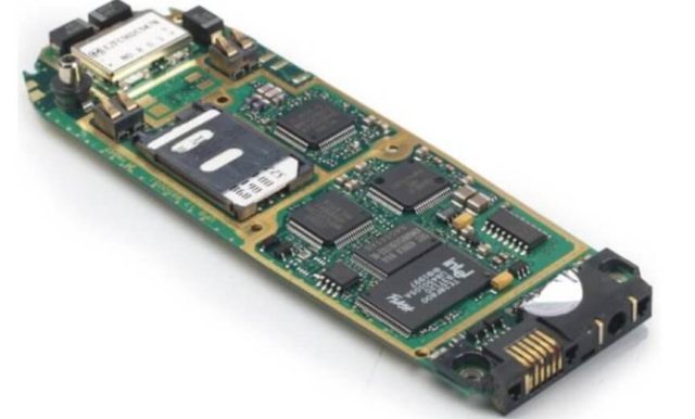
KKCPB implemented a complete smartphone PCB engineering optimization approach.
HDI Structure Optimization
Designed:
- 2+N+2 HDI structure
- Laser microvias
- Via-in-pad technology
- Fine-line routing
Signal Integrity Optimization
Applied:
- Differential pair matching
- Impedance simulation
- Reference plane optimization
- Crosstalk reduction
RF Performance Improvement
Implemented:
- RF isolation zones
- Ground via fences
- Optimized antenna routing
- Low-loss RF material selection
Thermal Optimization
Applied:
- Copper spreading layers
- Thermal via arrays
- Power plane optimization
Validation included:
- HFSS RF simulation
- ADS signal analysis
- TDR impedance testing
- Thermal FEM simulation
Measured Results
| Parameter | Target Requirement | KKCPB Result |
|---|---|---|
| Impedance Variation | ±5% | ±1.5% |
| Memory Signal Skew | <20ps | 12ps |
| RF Insertion Loss | <0.8dB | 0.48dB |
| EMI Reduction | Required | Improved 35% |
| HDI Microvia Yield | >95% | 98.7% |
| PCB Warpage | <0.15mm | 0.06mm |
Project Outcome
The optimized Mobile Phone PCB achieved:
- Higher signal integrity
- Improved 5G communication stability
- Better EMI performance
- Higher manufacturing yield
- Reduced thermal issues
The PCB successfully entered mass production for commercial 5G smartphones.
Stackup Design & RF Implementation
Representative 10-Layer HDI Smartphone PCB Stackup
| Layer | Function | Material |
|---|---|---|
| L1 | Component / RF Signal | High-Speed PCB Material |
| L2 | Ground Plane | Copper |
| L3 | High-Speed Signal | Low-Loss Material |
| L4 | Power Layer | Copper |
| L5 | Memory Signal | High TG PCB |
| L6 | Ground Plane | Copper |
| L7 | Processor Routing | HDI Material |
| L8 | Power Distribution | Copper |
| L9 | RF Signal Layer | Low Loss PCB |
| L10 | Bottom Component Layer | High Reliability PCB |
Simulation & Validation
HFSS Simulation
Used for:
- RF antenna interaction analysis
- EMI coupling evaluation
- Signal transmission optimization
ADS Simulation
Used for:
- High-frequency circuit modeling
- RF matching network optimization
TDR Testing
Used for:
- Differential impedance measurement
- Production consistency verification
Thermal FEM Simulation
Used for:
- Processor heat distribution
- Power component temperature analysis
Manufacturing Validation
Included:
- AOI inspection
- X-Ray inspection
- Microvia reliability testing
- Electrical testing
Environmental & Reliability Validation
| Test | Condition | Result |
|---|---|---|
| Thermal Cycling | -40°C ↔ +85°C, 1000 cycles | Passed |
| High Temperature Storage | 125°C, 1000h | Stable |
| Humidity Test | 85°C / 85% RH | No insulation failure |
| Drop Test Simulation | Mobile device impact condition | Passed |
| Solder Reflow | 260°C ×3 cycles | No delamination |
| Microvia Reliability Test | Thermal stress cycling | Passed |
These tests ensure smartphone PCB designs maintain stable electrical performance throughout product lifetime.
Engineering Summary
A successful Mobile Phone PCB Layout requires a combination of high-density manufacturing capability, RF engineering knowledge, signal integrity optimization, thermal design, and strict reliability control.
As smartphone technologies evolve toward 5G, AI processing, and advanced wireless communication, PCB designs must support higher data rates, smaller form factors, and greater power efficiency.
KKCPB provides professional PCB solutions for:
- Smartphone PCB
- 5G Antenna PCB
- HDI PCB
- RF PCB
- High-Speed PCB
- Multilayer PCB
- Prototype and Mass Production PCB
With expertise in HDI fabrication, RF PCB manufacturing, controlled impedance technology, simulation verification, and quality management, KKCPB helps global electronics companies develop reliable and high-performance mobile communication products.
