
Printed Circuit Board (PCB) layout and wiring are essential processes that transform a circuit schematic into a manufacturable electronic product. A well-designed PCB not only ensures electrical performance but also improves reliability, thermal management, production efficiency, and long-term stability.
As electronic products become smaller and more powerful, PCB designs face increasing challenges such as higher signal speeds, greater component density, and stricter reliability requirements. Improper layout or routing may result in issues including:
- Signal interference
- Voltage instability
- Excessive heat generation
- Electromagnetic compatibility (EMC) problems
- Manufacturing difficulties
Therefore, following fundamental PCB layout and wiring principles is essential for achieving a reliable design.
1. PCB Layout Planning Before Routing
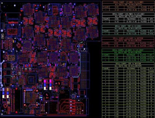
Before starting PCB routing, designers should develop an overall layout strategy based on circuit functions, signal characteristics, and manufacturing requirements.
Important planning considerations include:
- Functional block division
- Signal flow direction
- Power distribution structure
- Critical component placement
- Thermal management requirements
A good PCB layout should achieve:
- Shorter signal paths
- Clear functional separation
- Reduced interference
- Easier manufacturing and testing
2. Functional Block Partitioning
One of the basic principles of PCB layout is separating different circuit functions.
Typical functional areas include:
- Power supply section
- Analog circuit section
- Digital processing section
- RF communication section
- Interface and connector area
Keep Noisy Circuits Away from Sensitive Circuits
High-noise circuits such as:
- Switching power supplies
- Clock circuits
- High-current drivers
should be separated from sensitive circuits such as:
- Analog amplifiers
- Sensor interfaces
- RF circuits
This reduces electromagnetic coupling and improves signal quality.
3. Component Placement Rules
Component placement directly affects PCB performance and manufacturability.
Place Critical Components First
Priority should be given to:
- Main processors
- Power management ICs
- RF components
- High-speed interfaces
- Clock sources
These components determine the routing strategy and signal integrity performance.
Minimize Signal Path Length
Components connected by high-speed or sensitive signals should be placed close together.
Shorter connections help:
- Reduce transmission loss
- Minimize parasitic effects
- Improve signal integrity
Consider Assembly Requirements
Component placement should also support manufacturing processes:
- Maintain sufficient component spacing
- Consider SMT assembly direction
- Avoid uneven copper distribution
- Provide accessibility for inspection
4. PCB Routing Rules
Routing is one of the most important stages in PCB design.
Maintain Proper Trace Width
Trace width should be selected according to:
- Current carrying requirements
- Voltage levels
- Manufacturing capability
- Impedance requirements
Power traces usually require wider widths than signal traces.
Avoid Sharp Corners
Sharp 90-degree bends can create impedance discontinuities and affect signal performance.
Recommended practices include:
- Use 45-degree routing
- Use curved traces for high-frequency signals
- Maintain consistent trace width
Minimize Unnecessary Via Usage
Every via introduces parasitic effects.
Excessive vias may increase:
- Signal loss
- Manufacturing complexity
- Cost
For high-speed signals, layer transitions should be carefully controlled.
5. High-Speed Signal Routing Considerations
High-speed signals require additional design attention.
Controlled Impedance Design
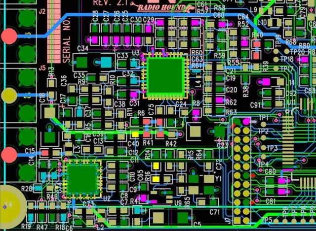
For high-speed and RF circuits, PCB traces must maintain controlled impedance.
Important factors include:
- Trace width
- Copper thickness
- Dielectric thickness
- PCB material properties
Common impedance requirements include:
- 50Ω single-ended signals
- 90Ω differential signals
- 100Ω differential signals
Differential Pair Routing
Differential signals should maintain:
- Equal trace length
- Consistent spacing
- Symmetrical routing
Common differential interfaces include:
- USB
- Ethernet
- LVDS
- PCIe
Proper differential routing reduces noise and improves signal integrity.
Clock Signal Routing
Clock signals are sensitive to interference.
Recommended practices:
- Keep traces short
- Avoid parallel routing with noisy signals
- Use proper termination methods
- Maintain reference planes
6. Power and Ground Design Rules
Power distribution is fundamental to PCB reliability.
Use Solid Ground Planes
A continuous ground plane provides:
- Stable current return paths
- Reduced EMI
- Improved signal integrity
Avoid unnecessary splits in high-speed signal return paths.
Place Decoupling Capacitors Properly
Decoupling capacitors should be placed:
- Close to IC power pins
- With short connection paths
- Near ground vias
This reduces power supply noise and improves circuit stability.
Separate High-Current Paths
High-current circuits should have dedicated routing strategies.
Examples include:
- Motor drivers
- Power amplifiers
- Battery charging circuits
Proper separation prevents interference with sensitive circuits.
7. Thermal Management Considerations
PCB layout should consider heat generation and dissipation.
Important thermal design methods include:
Copper Area Optimization
Large copper areas help distribute heat.
Thermal Vias
Thermal vias transfer heat between PCB layers and improve cooling efficiency.
Component Placement
High-power components should be positioned to avoid excessive heat concentration near sensitive devices.
8. EMC Design Rules
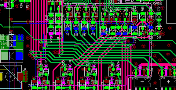
Good PCB layout contributes significantly to electromagnetic compatibility.
Reduce Current Loop Area
Smaller current loops reduce electromagnetic radiation.
Separate High-Frequency Noise Sources
Keep sources such as:
- Switching regulators
- Fast digital signals
- RF transmit circuits
away from sensitive areas.
Use Shielding When Necessary
For demanding applications, shielding structures may be used to improve EMC performance.
9. DFM (Design for Manufacturing) Considerations
A PCB design must not only work electrically but also be manufacturable.
Important DFM considerations include:
Minimum Trace and Spacing Requirements
Design rules should match PCB manufacturing capabilities.
Solder Mask and Pad Design
Proper pad design helps prevent:
- Solder bridging
- Component mounting defects
- Assembly issues
Testability
A good PCB design should include:
- Sufficient test points
- Accessible debugging interfaces
- Consideration for ICT and functional testing
10. PCB Layout Verification Before Production
Before manufacturing, PCB designs should undergo comprehensive review.
Common checks include:
Design Rule Check (DRC)
Verifies:
- Clearance
- Trace width
- Via rules
- Layer constraints
Signal Integrity Analysis
Used for:
- High-speed interfaces
- RF circuits
- Critical timing signals
Thermal and EMC Analysis
Helps identify potential reliability issues before production.
Common PCB Layout and Wiring Mistakes
Some frequent design problems include:
- Routing sensitive signals near noisy circuits
- Incorrect grounding methods
- Excessive trace length
- Poor power distribution
- Insufficient component spacing
- Ignoring manufacturing limitations
Avoiding these mistakes during early design stages can significantly reduce debugging time and production risks.
Conclusion
PCB layout and wiring are fundamental to achieving reliable electronic products. A successful PCB design requires careful consideration of component placement, routing strategy, power distribution, signal integrity, EMC performance, thermal management, and manufacturing requirements.
By following basic PCB layout rules and applying proper design practices, engineers can improve product reliability, reduce production issues, and create PCBs that meet both electrical and manufacturing expectations.
