
With the continuous development of high-speed electronics, modern PCB designs are becoming increasingly complex. Higher data rates, faster signal transitions, and more compact product structures have made signal integrity a critical factor in electronic system performance.
In traditional low-speed PCB applications, traces are mainly considered simple electrical connections. However, when signal frequencies increase, PCB traces behave as transmission lines, and their electrical characteristics directly affect signal quality.
Among these characteristics, impedance control is one of the most important aspects of PCB design and manufacturing.
Improper impedance control may result in:
- Signal reflection
- Transmission loss
- Crosstalk
- Timing errors
- Electromagnetic interference (EMI)
- System instability
Therefore, maintaining consistent impedance throughout PCB design and manufacturing is essential for ensuring reliable signal transmission.
1. What Is PCB Impedance?
1.1 Definition of PCB Impedance
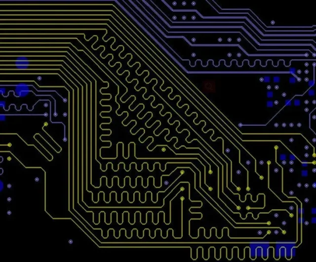
PCB impedance refers to the opposition experienced by a high-frequency signal when traveling through a PCB transmission line.
Unlike DC resistance, impedance is affected by both:
- Resistance
- Capacitance
- Inductance
It depends on the interaction between:
- Copper trace geometry
- PCB dielectric material
- Signal frequency
- Reference plane structure
1.2 Common Types of PCB Impedance
Single-Ended Impedance
Single-ended impedance refers to the impedance of an individual signal trace relative to a reference plane.
Common applications:
- Clock signals
- Control signals
- RF transmission lines
A typical value is:
- 50Ω impedance
Differential Impedance
Differential impedance refers to the impedance between two coupled signal traces.
Common applications:
- USB
- Ethernet
- PCIe
- LVDS
- High-speed communication interfaces
A common value is:
- 90Ω–100Ω differential impedance
2. Why Is Impedance Important in PCB Design?
2.1 Maintaining Signal Integrity
As signal speed increases, impedance mismatch can cause signal reflections.
When the transmitted signal encounters a sudden impedance change:
- Part of the signal energy reflects back
- The waveform becomes distorted
Potential consequences include:
- Data errors
- Reduced communication reliability
- System malfunction
Controlled impedance ensures that signals travel smoothly through the PCB.
2.2 Reducing Signal Loss
High-frequency signals experience greater transmission loss due to:
- Dielectric loss
- Copper loss
- Surface roughness effects
Proper impedance design helps optimize:
- Signal attenuation
- Transmission efficiency
- Overall system performance
2.3 Improving Electromagnetic Compatibility (EMC)
Poor impedance control can increase:
- Signal radiation
- Electromagnetic interference
Stable impedance helps:
- Reduce unwanted emissions
- Improve noise immunity
- Enhance system compliance
2.4 Ensuring High-Speed Interface Reliability
Modern electronic systems rely on high-speed interfaces such as:
- DDR memory
- USB
- PCIe
- Ethernet
- RF communication modules
These interfaces require strict impedance control to achieve reliable operation.
3. Factors Affecting PCB Impedance
3.1 Trace Width
Trace width directly influences impedance.
General relationship:
- Wider trace → Lower impedance
- Narrower trace → Higher impedance
During design, engineers must balance:
- Electrical requirements
- Current carrying capability
- Manufacturing limitations
3.2 Copper Thickness
Copper thickness affects the cross-sectional area of the conductor.
Factors include:
- Copper weight
- Electroplating thickness
- Manufacturing variation
Changes in copper thickness can cause impedance deviation.
3.3 Dielectric Thickness
The distance between the signal layer and reference plane affects impedance.
A smaller dielectric thickness generally results in:
- Lower impedance
A larger dielectric thickness generally results in:
- Higher impedance
Accurate stack-up design is essential for impedance control.
3.4 Dielectric Constant (Dk)
The PCB material dielectric constant affects signal propagation.
Important considerations include:
- Dk stability
- Frequency dependency
- Temperature variation
High-frequency applications often require materials with stable electrical characteristics.
3.5 Trace Geometry
Other factors affecting impedance include:
- Trace shape
- Copper roughness
- Trace spacing
- Via structures
Even small geometry changes may influence high-frequency performance.
4. Impedance Control in PCB Design
4.1 Stack-Up Design
A proper PCB stack-up is the foundation of impedance control.
Engineers need to define:
- Signal layers
- Ground layers
- Power layers
- Dielectric materials
- Layer spacing
A stable reference plane helps maintain predictable impedance.
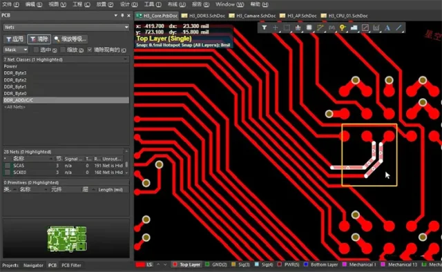
4.2 Controlled Impedance Routing
During PCB layout, engineers should maintain:
- Consistent trace width
- Stable spacing
- Continuous reference planes
Avoid:
- Sudden trace width changes
- Excessive vias
- Routing across plane gaps
4.3 Differential Pair Design
Differential signals require careful control of:
- Pair spacing
- Trace length matching
- Routing symmetry
Incorrect differential routing can cause:
- Mode conversion
- Noise increase
- Signal degradation
5. Impedance Considerations During PCB Manufacturing
5.1 Material Selection
Manufacturers must select materials according to application requirements.
Examples:
Standard Applications
- FR-4 materials
High-Speed Applications
- Low-loss FR-4
- Rogers materials
- PTFE-based laminates
Material selection affects:
- Dielectric performance
- Signal loss
- Impedance accuracy
5.2 Manufacturing Tolerances
Actual impedance may vary due to:
- Etching variation
- Copper thickness deviation
- Lamination variation
- Material tolerance
Professional PCB manufacturing requires strict process control.
5.3 Layer Alignment Accuracy
For multilayer PCBs, misalignment between layers can affect:
- Trace geometry
- Reference plane distance
- Final impedance
High-density PCB manufacturing requires precise registration control.
6. Impedance Testing and Verification
6.1 TDR (Time Domain Reflectometry) Testing
TDR is commonly used to verify PCB impedance.
It measures:
- Actual impedance value
- Signal reflection characteristics
- Transmission consistency
6.2 Test Coupon Verification
Manufacturers often include impedance test coupons in PCB panels.
These coupons help confirm:
- Process stability
- Manufacturing accuracy
- Compliance with design requirements
6.3 Engineering Validation
Before mass production, prototype validation helps evaluate:
- Signal performance
- Interface stability
- System reliability
7. Applications Requiring Impedance Control
7.1 High-Speed Communication Systems
Applications:
- Data centers
- Network equipment
- Communication devices
Requirements:
- Low signal loss
- Stable transmission
7.2 RF and Microwave PCB
Applications:
- Wireless modules
- Radar systems
- Satellite communication
Requirements:
- Precise impedance control
- Low insertion loss
- Phase stability
7.3 Automotive Electronics
Applications:
- ADAS systems
- Radar sensors
- Vehicle communication modules
Requirements:
- Long-term reliability
- Environmental stability
7.4 Semiconductor Test Equipment
Applications:
- ATE load boards
- High-speed testing interfaces
Requirements:
- Accurate signal measurement
- Repeatable electrical performance
8. Common Impedance Control Problems
Incorrect Stack-Up Design
Problem:
The actual PCB structure differs from simulation assumptions.
Impact:
- Impedance deviation
- Signal integrity issues
Inconsistent Trace Width
Problem:
Uneven etching or routing changes.
Impact:
- Reflection
- Signal distortion
Poor Reference Plane Design
Problem:
Interrupted return paths.
Impact:
- Increased EMI
- Reduced signal quality
Ignoring Manufacturing Capability
Problem:
Design exceeds fabrication limits.
Impact:
- Low yield
- Higher production cost
9. Best Practices for PCB Impedance Control
To achieve reliable impedance performance, engineers should:
During Design
- Define impedance requirements early
- Select suitable PCB materials
- Optimize stack-up structure
- Maintain controlled routing rules
During Manufacturing
- Control material parameters
- Monitor process variation
- Perform impedance testing
- Validate prototype performance
During Production
- Maintain process consistency
- Perform quality inspection
- Monitor critical electrical parameters
Conclusion
Impedance control is a fundamental element of modern PCB design and manufacturing, especially for high-speed, RF, and advanced electronic systems.
Achieving reliable impedance performance requires coordination between:
- PCB designers
- Material suppliers
- PCB manufacturers
- Testing engineers
By controlling stack-up design, trace geometry, material selection, and manufacturing processes, engineers can reduce signal integrity risks and improve overall product reliability.
As electronic systems continue moving toward higher frequencies and faster data rates, impedance control will remain a key technology for developing high-performance PCB solutions.
