HomeAuthor

kkpcb02 - KKPCB - Page 7 of 15

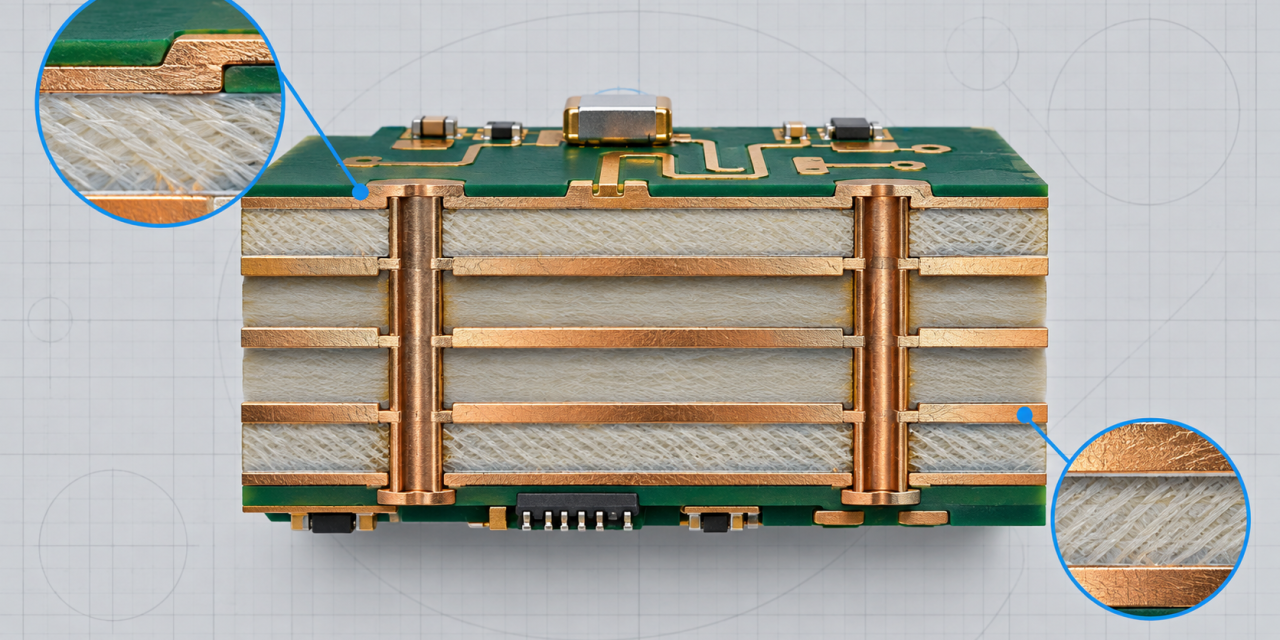
RO4003C PCB Stackup Release: Managing Dielectric Thickness in Compact RF Modules

Compact RF modules often fail between schematic approval and fabrication release because the RO4003C PCB stackup is treated as a static drawing. Resin content, copper thickness, press-out, and reference-plane choices change the field geometry that the RF model used. A controlled RO4003C PCB stackup release turns those assumptions into a buildable document for engineering and...

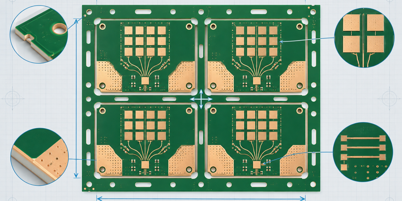
RO4003C PCB Panelization for 5G Antenna Arrays: Controlling Phase Consistency and RF Yield

When a 5G antenna array moves from prototype to volume production, the difficult question is rarely whether the RF layout works once. The risk is whether every unit on a panel keeps the same phase center, launch geometry, and return-current path after imaging, lamination, plating, routing, and singulation. A disciplined RO4003C PCB panelization plan makes...

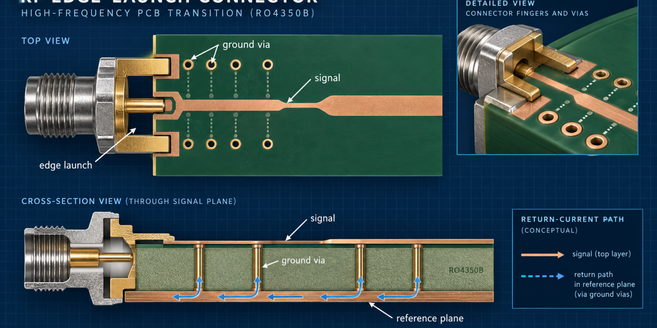
RO4350B PCB RF Edge Launch: Surface Finish and Connector Reliability

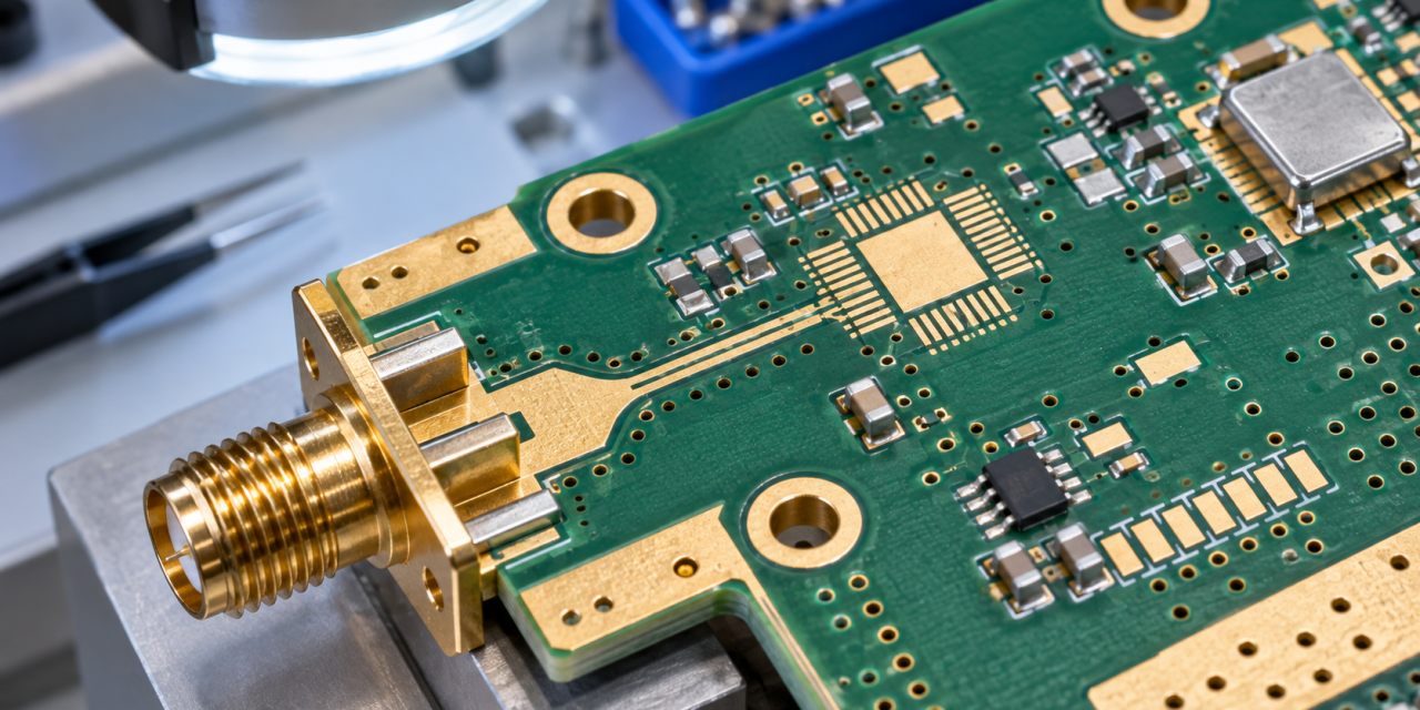
RF edge launches are often tuned electrically and then weakened by a small production detail: an uncontrolled surface finish, a connector land that changes during etch, or a ground transition that does not meet the enclosure. This guide uses the RO4350B PCB to organize an edge-launch review around electrical intent, finish selection, and repeatable inspection....

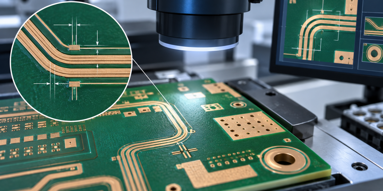
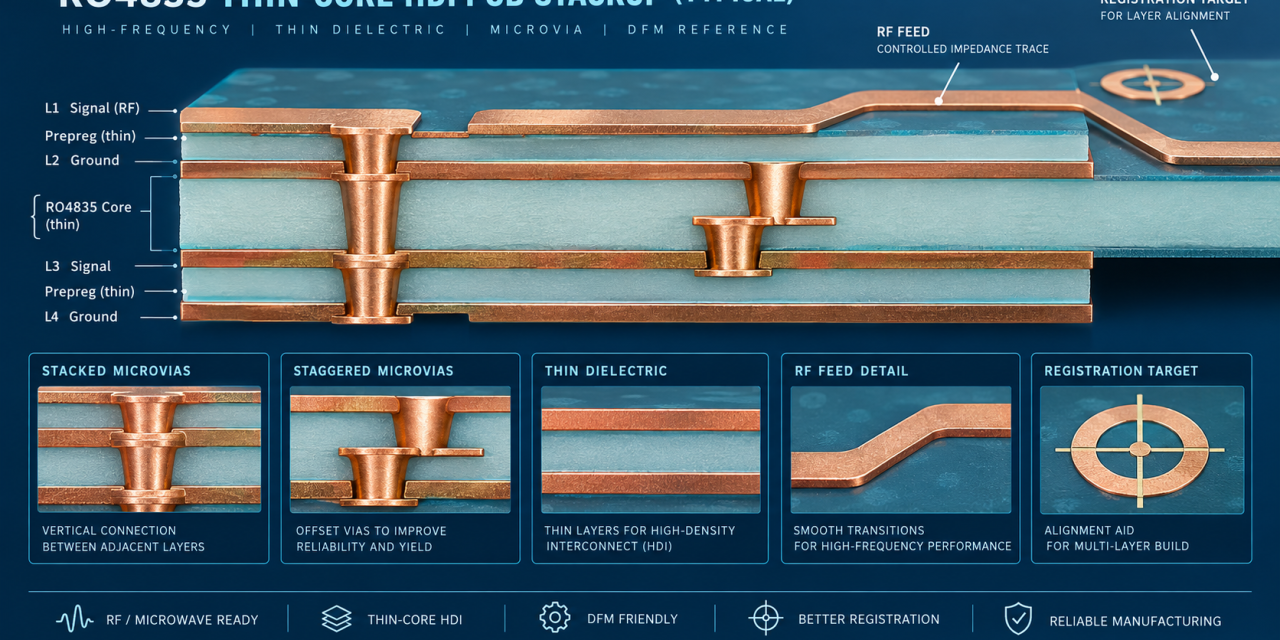
RO4835 PCB HDI Microvia Design for Thin Radar Modules

Thin radar modules often force an uncomfortable trade-off: the RF launch wants a stable reference plane while the mechanical envelope pushes the stackup toward finer features. This engineering guide uses the RO4835 PCB to explain how an HDI build can be reviewed without confusing design intent with measured qualification data. Define the thin-module constraint first...