
Automotive Module PCB — Fabrication can meet a drawing and assembly can still move the electrical result. Paste height, reflow warpage, shield force, cleaning chemistry, heat spreaders, and connector rework all act on vehicle modules that package communication, power, sensing, and control functions behind a connector-rich housing with tight mechanical and service constraints. This production guide turns the Automotive Module PCB assembly flow into measurable controls so a pilot lot provides evidence instead of a generic “assembly passed” label. The release must make a distinction between a design target, a supplier typical value, an engineering range, and a measured value.
The steps below are a new engineering narrative for this product family, not a customer measurement or a copied case study.
Keep the Automotive Module PCB record joined to the drawing, stackup, fabrication note, assembly recipe, and verification plan. The same physical path should be named in every document so a late sourcing or housing change cannot quietly alter the vehicle behavior.
Automotive Module PCB — Map heat, force, and sensitive geometry
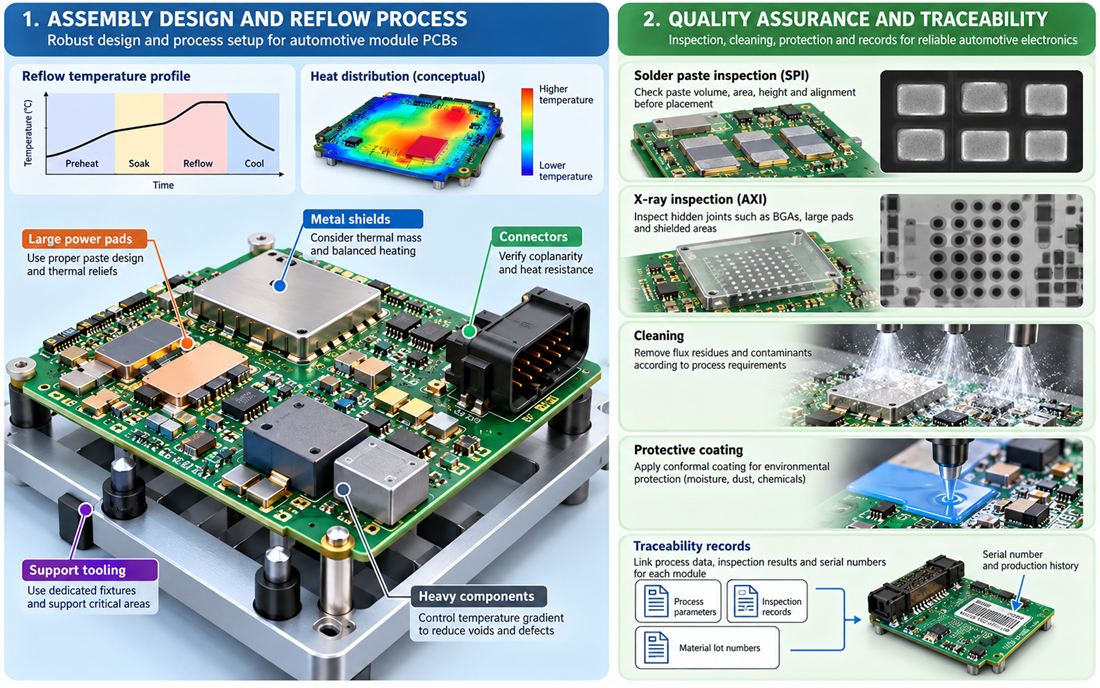
Mark the heat sources, large exposed pads, thin edges, connector zones, sensor apertures, and support points on the assembly drawing. An uneven copper pattern can pull a board during reflow; a stiff shield or heat spreader can add force after cooling. For Automotive Module PCB, the thermal path from component to copper, dielectric, carrier, and housing should be discussed with the mechanical and RF owners before stencil release. The program file should cross-reference high-reliability PCB and RF PCB so design and sourcing see the same boundary. The released Automotive Module PCB page is an internal capability reference; the engineering decision remains in this article and the project file.
Control paste and reflow around the RF path
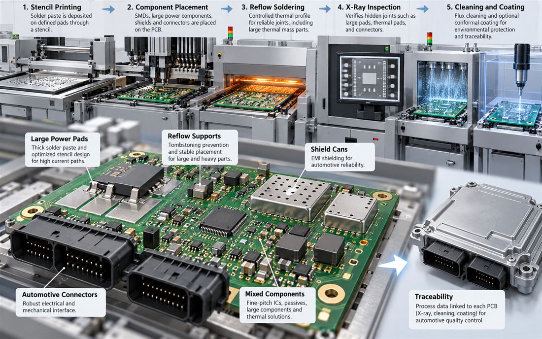
Control print volume, stencil reductions, soak and peak ranges, conveyor profile, and allowed reflow passes. Excess solder can wick toward a launch or change connector coplanarity; insufficient solder can raise contact resistance or weaken a thermal joint. The PCB assembly work instruction should flag components that must not be reheated close to a sensor or RF transition. The handoff should name thermal management PCB, via design, and surface finish PCB where those terms describe a controlled physical feature. The released Automotive Module PCB page is an internal capability reference; the engineering decision remains in this article and the project file.
Choose cleaning and coating with the material
Cleaning and coating are electrical decisions as well as cosmetic ones. Flux residue, ionic contamination, solvent attack, and moisture trapped under a shield can change high-impedance nodes or bond strength. Select no-clean, aqueous, or solvent cleaning with the laminate, solder mask, adhesive, and conformal-coating plan in view. The PCB materials record should state the material compatibility and drying condition used for the pilot. Keep turnkey PCB assembly beside the drawing revision and assign PCB materials as the verification owner. The released Automotive Module PCB page is an internal capability reference; the engineering decision remains in this article and the project file.
Inspect the features that carry system risk
Pair AOI with the inspection that matches the risk: X-ray for hidden joints and voids, coplanarity checks for connectors, cross-sections for internal vias, and a functional screen that exercises the actual bus, sensor, or RF path. For a radar or high-frequency board, a low-frequency continuity pass does not prove phase or loss. Tie the result to the PCB manufacturing lot and the exact assembly revision. The traveller can connect high frequency PCB design with controlled impedance PCB and preserve evidence for the next lot. The released Automotive Module PCB page is an internal capability reference; the engineering decision remains in this article and the project file.
Keep lot evidence connected to the board revision
Keep stencil revision, paste lot, oven profile, inspection records, rework log, cleaning batch, and disposition of every RF- or sensor-related defect. If a board was reworked twice, the release record must say so. This evidence lets a project manager distinguish a stable process window from a lucky first-pass unit and gives the next lot a clear escalation path. Before sign-off, confirm PCB manufacturing and PCB assembly use the same revision and acceptance method.
Release checklist for the next vehicle build
- State the vehicle interface, operating band, and environmental boundary for Automotive Module PCB.
- Identify the controlled material construction, copper profile, and pressed dielectric tolerance.
- Show the signal and return path through connectors, vias, shields, planes, and housing datums.
- Tie fabrication and assembly checks to a revisioned drawing, coupon, or inspection record.
- Label typical values, design targets, engineering ranges, and measured values separately.
- Record the owner and closure evidence for each open RF, thermal, mechanical, and service risk.
Sources: Analog Devices mixed-signal and power-layout guidance; Würth automotive connector and signal-integrity application notes; Rogers hybrid automotive PCB guidance; and Qorvo RF integration material. These authoritative engineering references inform the reasoning; no external link is inserted into the article and no customer measurement, certification, or simulation result is implied without retained project evidence.
