HomeAuthor

kkpcb02 - KKPCB - Page 8 of 15

RO4350B PCB Stackup Selection for 5G and Microwave Mixed-Signal Boards

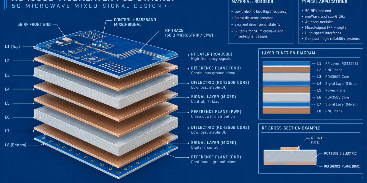
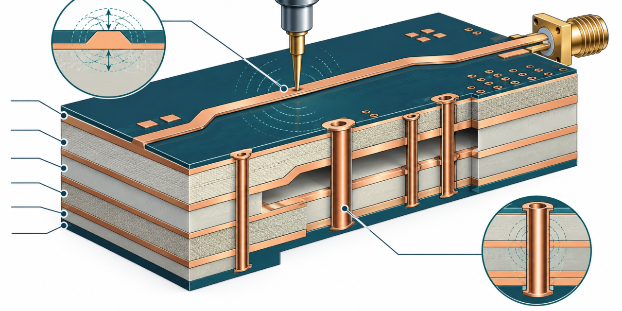
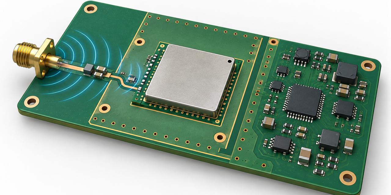
When a radio board combines a 5G front end, clock distribution, and digital processing, stackup selection becomes a system decision rather than a material shortcut. An RO4350B PCB can provide a predictable RF foundation, but only when the chosen dielectric thickness, copper, reference planes, and mixed-signal boundary are carried consistently into fabrication. This guide gives...

RO4835 PCB Stackup Decisions for 77 GHz Radar Phase Stability

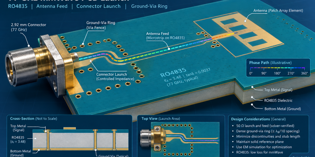
At millimeter-wave frequencies, a small dielectric or registration change can move the phase of an antenna feed enough to reduce array margin. The practical question is not simply whether an RO4835 PCB is low loss; it is how the stackup, copper geometry, and fabrication handoff keep phase repeatable from prototype to production. This engineering guide...

RO3003 PCB Thermal Design for High-Power RF Modules

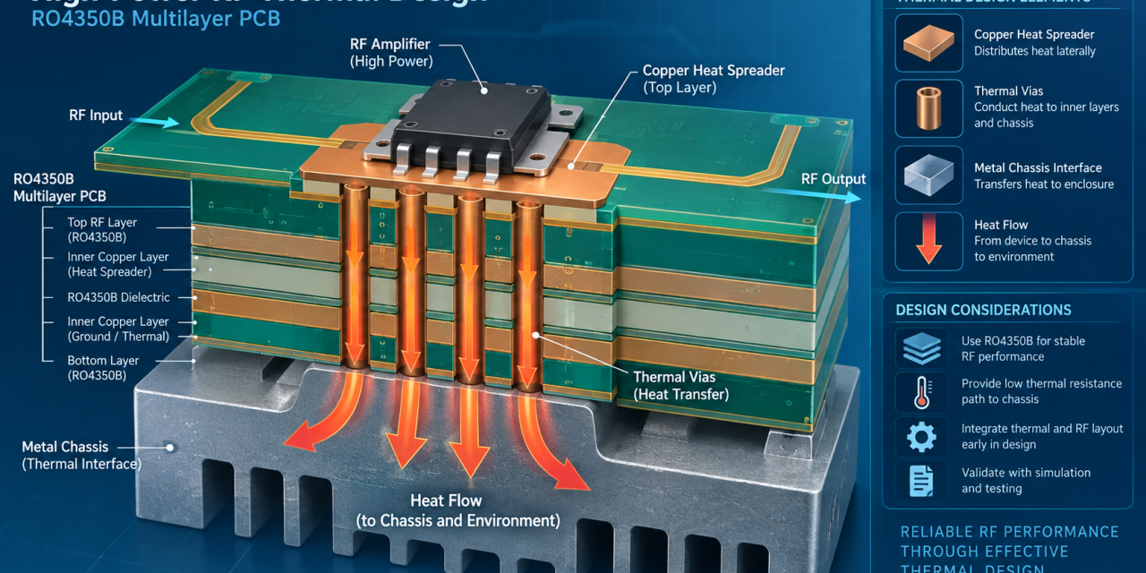
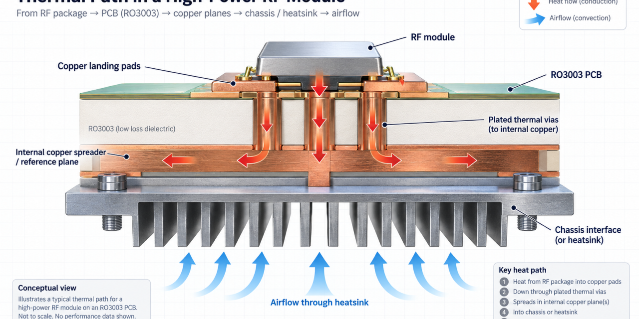
Engineering intent. High-power RF modules combine heat, current, and microwave loss in a small area. This article presents a practical workflow for using an RO3003 PCB as part of a thermal-aware RF module. It is a design guide, not a customer case study or a measured KKPCB result. RO3003 is a ceramic-filled PTFE laminate in...

RO3003 PCB Phased-Array Feed Network Layout

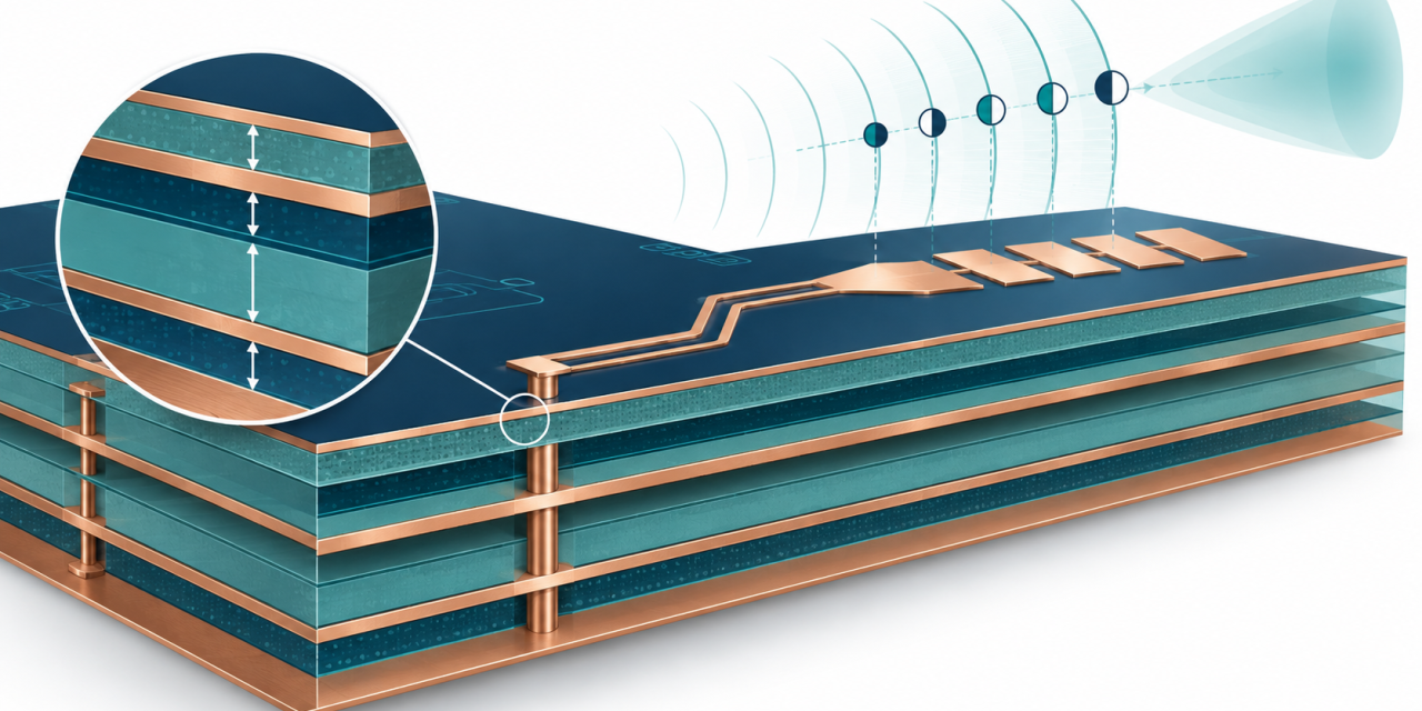
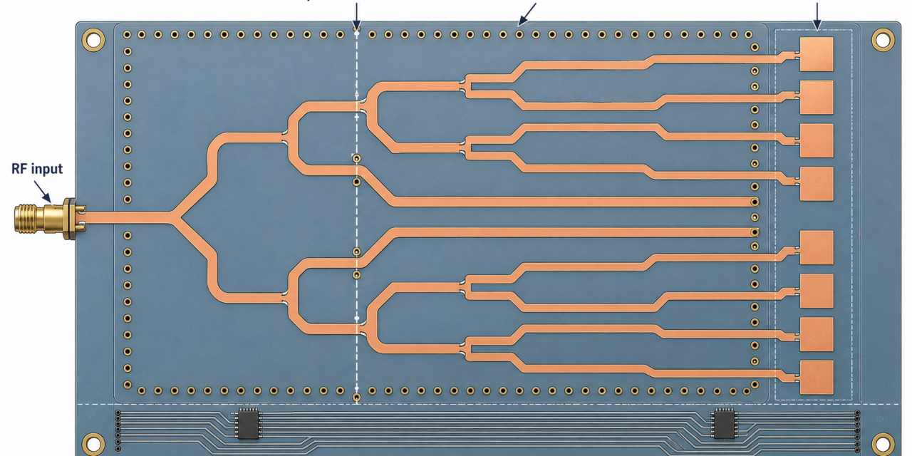
Engineering intent. A phased array can lose beam accuracy when equal-looking traces have different electrical lengths or transitions. This article explains how to plan an RO3003 PCB feed network for a conceptual phased-array module. It separates layout targets from measured production data and does not claim a KKPCB customer case study. RO3003 belongs to the...