
Table of Contents
A LoRa PCB gateway can appear to have a healthy radio, a valid firmware image, and a correctly tuned antenna yet lose sensitivity after the enclosure, cable, or mounting hardware changes. The common project mistake is to treat the board as a passive carrier for the radio module. A long-range gateway is a coupled system: the antenna boundary, chassis, coax launch, ground return, and shield datum all participate in the RF environment. When one of those boundaries moves, the receive margin can fall even though the schematic is unchanged.
The gateway symptom that points to the board
For a field gateway, the first clue is often not a failed conducted test. It is a shortened range at one mounting orientation, a larger spread between units, or a link that recovers when the lid is loosened. A LoRa PCB can show this behavior when its reference plane ends near the antenna, when a mounting hole interrupts the return current, or when a coax pigtail is routed across a split in the chassis ground.
Before changing matching values on a LoRa PCB, separate the variables. Record the enclosure, antenna, cable length, board revision, mounting torque, and software configuration for every RF comparison. A practical RF PCB design review then asks whether the board edge and the enclosure datum are repeatable. If the prototype used a plastic cover and the pilot build uses coated metal, the same matching network no longer represents the same electromagnetic boundary.
For project managers, this distinction prevents a late “radio sensitivity” escalation from becoming an uncontrolled component change. The engineering team can first freeze mechanical datums, then adjust the RF network only after the board-to-enclosure geometry is stable.
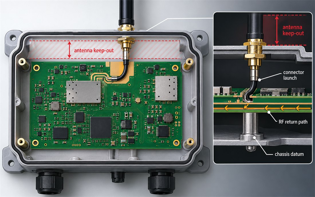
Freeze the antenna boundary and return path
For a LoRa PCB, the antenna region should be defined on more than the copper layer. Mark the keep-out on the fabrication drawing, assembly drawing, enclosure drawing, and inspection view. A LoRa PCB operating at sub-GHz frequencies may tolerate a longer trace than a microwave board, but it still depends on a predictable reference plane and a clean current path. The lower frequency does not make a discontinuous ground boundary harmless.
Use the enclosure as a controlled RF datum
Keep the antenna edge, metal wall, gasket, and standoff locations tied to one datum scheme. A screw head or conductive coating that moves into the keep-out can add capacitance at the exact point where the antenna was tuned. If the enclosure must change, issue a controlled drawing revision and repeat the same orientation matrix rather than relying on a single “best” orientation.
Ground stitching should support the intended return path, not form a decorative row of vias. On a LoRa PCB, place stitching where it closes the current loop around the launch and shields sensitive digital routes from the RF edge. Avoid placing a via fence through an antenna clearance zone or across a slot that the antenna uses as part of its field.
Protect the power and digital zones
A gateway often combines a high-current processor, Ethernet or cellular circuitry, and a low-noise receiver. Keep the regulator switch node, crystal, and high-speed memory away from the antenna feed. Use a defined solder mask boundary and document whether the antenna edge is coated. A surface finish decision should not silently change the exposed copper or add a meniscus inside the keep-out.
Control the connector launch and panel edge
The coax launch is a mechanical and RF interface. The connector footprint, pad relief, ground-via pattern, and cable exit direction should be released together. A LoRa PCB package that shows only the top copper can hide a drill-to-copper risk or a back-drill assumption that the shop cannot hold. Add a cross-section note for the launch, the intended reference plane, and the acceptable solder-mask opening.
Panelization introduces a second boundary for the LoRa PCB. Keep the RF edge away from routed rails, breakaway tabs, and tooling holes. A LoRa PCB fixture may need a support point near the connector, but the support cannot press on the antenna keep-out or force the board to bow. If the board is depanelized after reflow, define the cut direction and inspect the plated edge for burrs or exposed copper that can approach the antenna.
Use one representative impedance coupon and one launch witness structure when the board is panelized. They are not a substitute for system verification; they are evidence that the released geometry and stackup were built as intended. The coupon callout belongs in the DFM release package so that fabrication, assembly, and RF teams use the same revision.
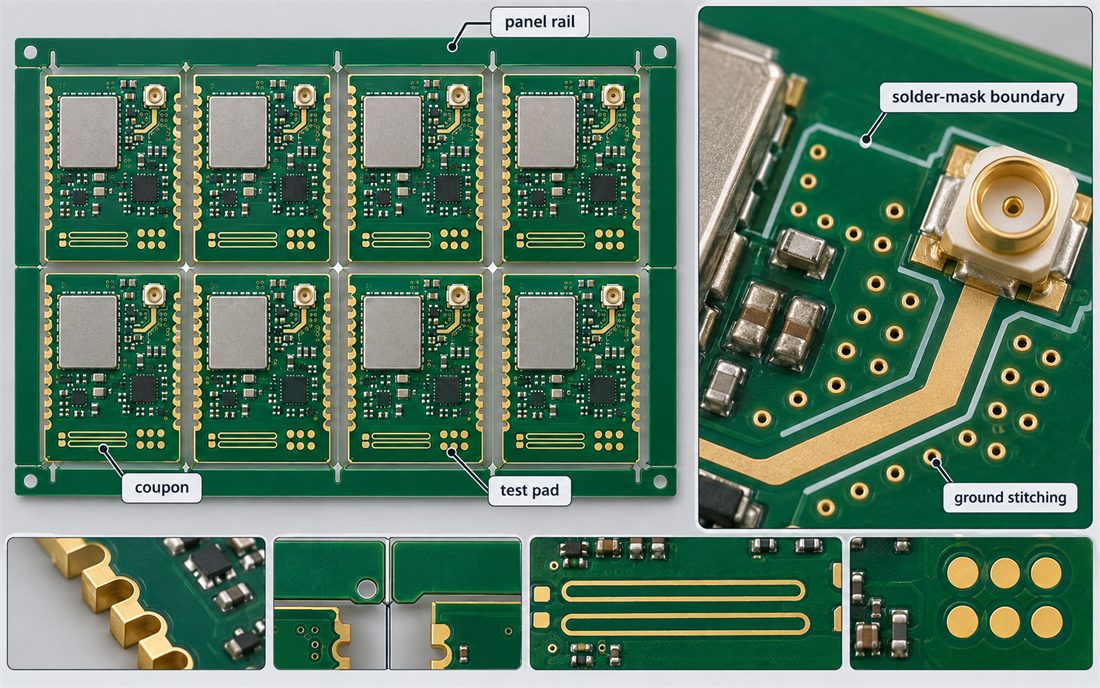
Release a repeatable gateway build
For a LoRa PCB gateway release, a reliable package makes the environmental and mechanical state visible. Include the stackup, dielectric assumptions, copper weights, antenna keep-out, connector part number, enclosure datum, coating mask, and panel drawing. The RF laminate selection should be tied to the actual thickness and process route; do not let a substitute material enter through a generic “equivalent” note without reviewing the antenna boundary and tuning plan.
At first article, inspect the antenna edge, connector launch, via fence, mask opening, and enclosure contact points. A registration check should confirm that the copper and mask are centered relative to the mechanical datum. During assembly, record the reflow profile, shield seating, cleaning route, and any rework around the RF path. A rework control note is important because a replacement connector or lifted shield can change the local return current.
For production monitoring, compare a small set of repeatable indicators: board outline and edge burrs, connector coplanarity, antenna keep-out cleanliness, and the configuration of the test fixture. A return-path review is especially useful after a component relocation. If the product uses a metal housing, keep the housing torque and gasket compression in the build record rather than leaving them to operator judgment.
When a LoRa PCB design revision is required, use a change table that identifies the affected RF boundary, the affected manufacturing operation, and the verification needed before release. The surface-finish specification, panel drawing, and inspection plan should all carry the same revision code. A final KKPCB production change-control review can then decide whether the change needs a new coupon, a new fixture, or a full antenna re-tune.
Sources: Taconic and Rogers laminate data sheets, Semtech LoRa radio application guidance, connector manufacturer launch recommendations, and KKPCB internal DFM and RF release practices were used as engineering references. Numerical statements in this article are design guidance or process targets, not a claim of a customer measurement.
