HomeTag

satellite PCB - KKPCB

Satellite PCB Launch Vibration: Keeping Board Resonance and Connector Loads in Check

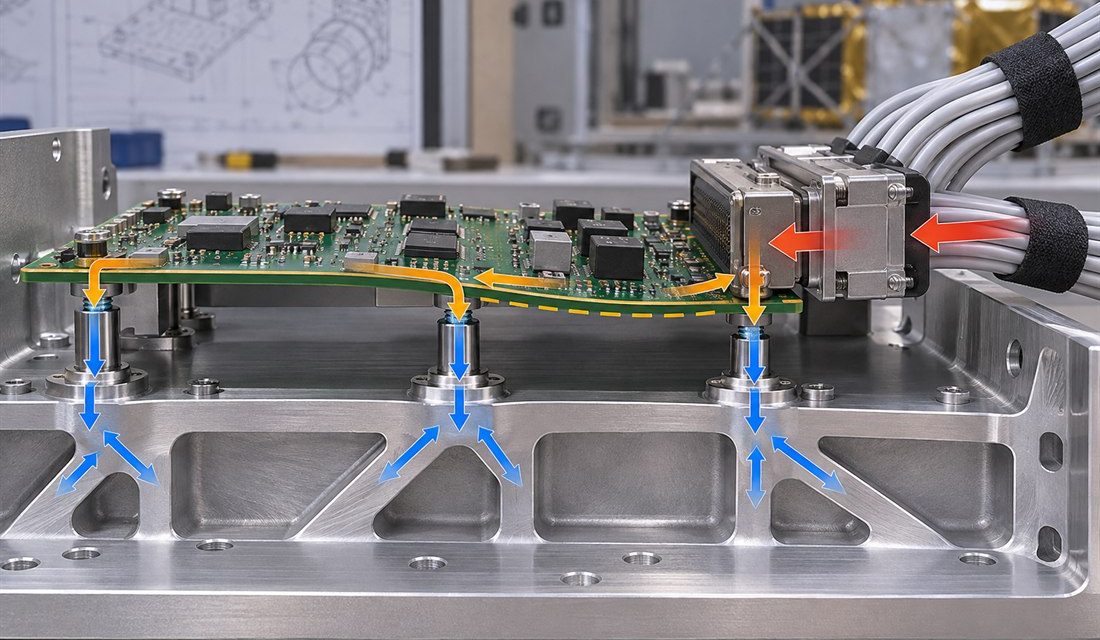
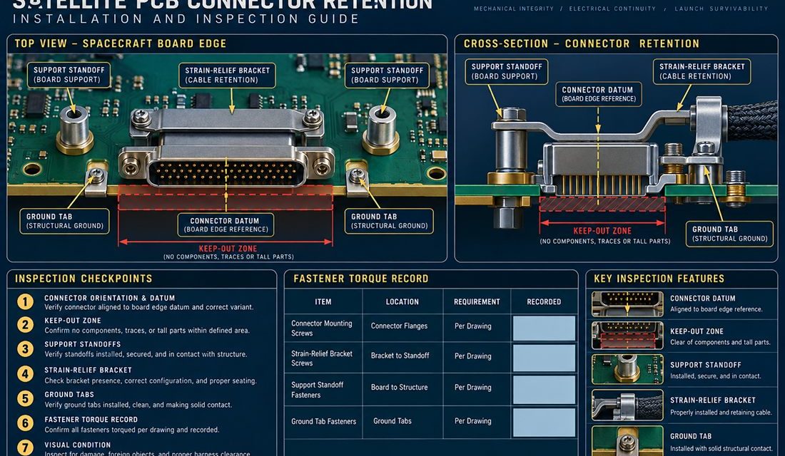
A launch environment turns a seemingly rigid electronics box into a coupled mechanical system. The spacecraft structure, chassis, mounting hardware, board, connectors, cable harness, and component masses all exchange load. If a Satellite PCB is treated as a bare laminate rather than a mounted assembly, the first resonance or a heavy connector can concentrate strain...
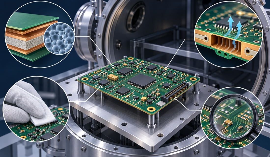
Satellite PCB Vacuum Reliability: Manage Outgassing, Cleanliness, and Material Controls

A Satellite PCB can pass electrical inspection on the bench and still become a contamination source after launch. In vacuum, volatile compounds have no convective path away from the assembly; they migrate and may condense on colder optical, RF, thermal-control, or detector surfaces. The engineering question is therefore not simply whether a laminate has a...

Satellite PCB Ku-Band Feed Networks: Preserving Phase Balance from Launch to Antenna

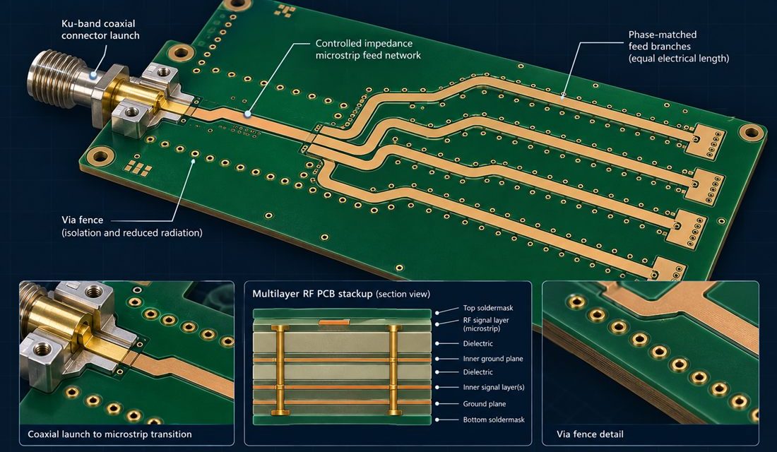
A Satellite PCB Ku-band feed network is often released as a routing problem, then fails as an integration problem. The electrical design may show equal-length branches and an acceptable nominal impedance, yet the assembled payload can lose phase balance when a connector launch, via fence, housing wall, or harness datum moves the return path. At...

Satellite PCB Thermal Drift: Managing CTE, Copper Density, and Chassis Interfaces

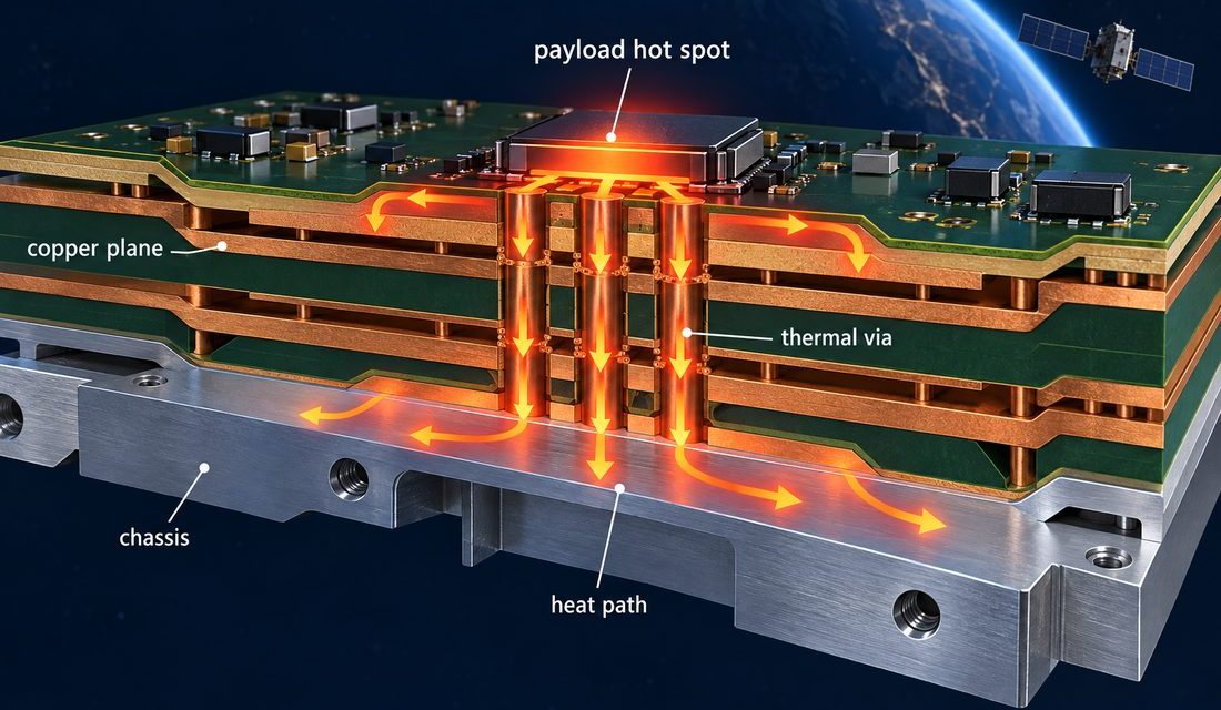
Satellite PCB thermal drift becomes a mission risk when a board is treated as a flat electrical drawing instead of a constrained mechanical and thermal assembly. A payload can meet its schematic targets and still show connector strain, oscillator frequency movement, or intermittent solder fatigue after repeated hot-cold transitions. This Satellite PCB thermal drift problem...

Satellite PCB Radiation Design for LEO Avionics: Dielectrics, Planes, and Shielded Returns

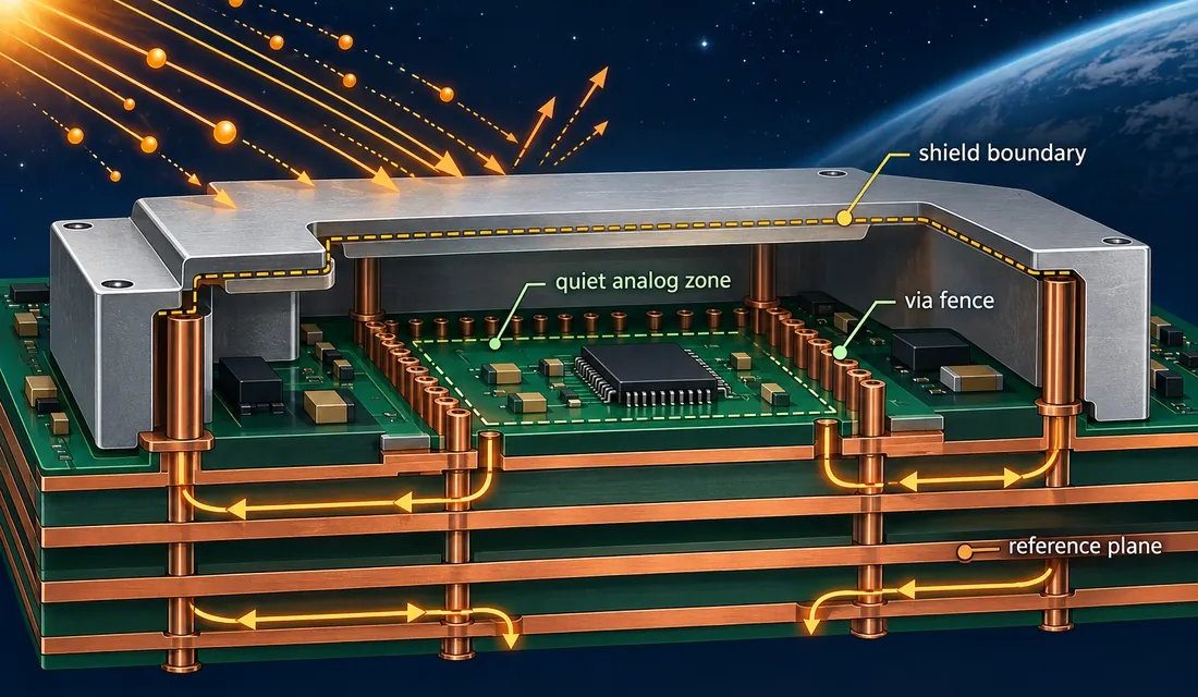
Satellite PCB radiation design for low-Earth-orbit avionics is often reviewed too late as a materials choice. The difficult question is not whether a board can route a signal; it is whether the dielectric, copper stack, enclosure bond, and return current still behave predictably after radiation exposure, thermal cycling, launch handling, and repeated engineering changes. A...

Ku/Ka Satellite PCB Launch Design: Taming Connector and Via Transitions at 30 GHz

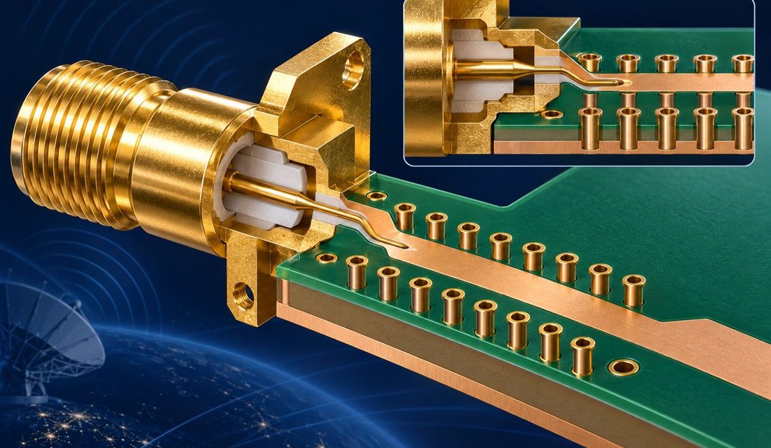
For Satellite PCB launch design, a Ku/Ka payload can meet its schematic targets and still lose margin at the board edge. The connector, launch pad, reference plane, via field, and enclosure datum form one electromagnetic interface. The Satellite PCB release must hold that board-to-enclosure datum constant across design and manufacturing. At 30 GHz, even a...

Satellite PCB: High-Reliability PCB Solutions for Aerospace and Space Communication Systems

The Growing Importance of Satellite PCB Technology Modern satellite and aerospace systems are rapidly advancing toward: High-speed space communication Global satellite networking Deep-space exploration AI-powered aerospace systems High-frequency radar and sensing platforms Satellite electronics now support: Navigation systems RF communication payloads Earth observation platforms Aerospace control systems Military communication networks These complex systems require highly...

Satellite PCB: High-Reliability PCB Design for Space and Satellite Communication Systems

1. Introduction: The Role of Satellite PCB in Space Technology Satellite systems operate in one of the most extreme environments in engineering, including: Vacuum conditions Extreme temperature cycling High radiation exposure Long-term mission lifetimes without maintenance Because of these conditions, Satellite PCB design must meet extremely strict reliability, thermal, and electrical performance requirements. Modern satellite...