
Automotive High Frequency PCB — The connector, coax, antenna, sensor flex, or board edge is where a schematic becomes a three-dimensional part. In high-frequency automotive radar and connectivity boards where fast edges, 76–81 GHz channels, and a constrained metal housing share the same release, that interface also has to survive mating force, housing tolerances, and service handling. This Automotive High Frequency PCB guide treats the transition as a controlled subassembly: its datum, launch geometry, return path, inspection method, and substitute-part rule are all released together. The release must make a distinction between a design target, a supplier typical value, an engineering range, and a measured value.
The steps below are a new engineering narrative for this product family, not a customer measurement or a copied case study.
Keep the Automotive High Frequency PCB record joined to the drawing, stackup, fabrication note, assembly recipe, and verification plan. The same physical path should be named in every document so a late sourcing or housing change cannot quietly alter the vehicle behavior.
Automotive High Frequency PCB — Set the mechanical datum first
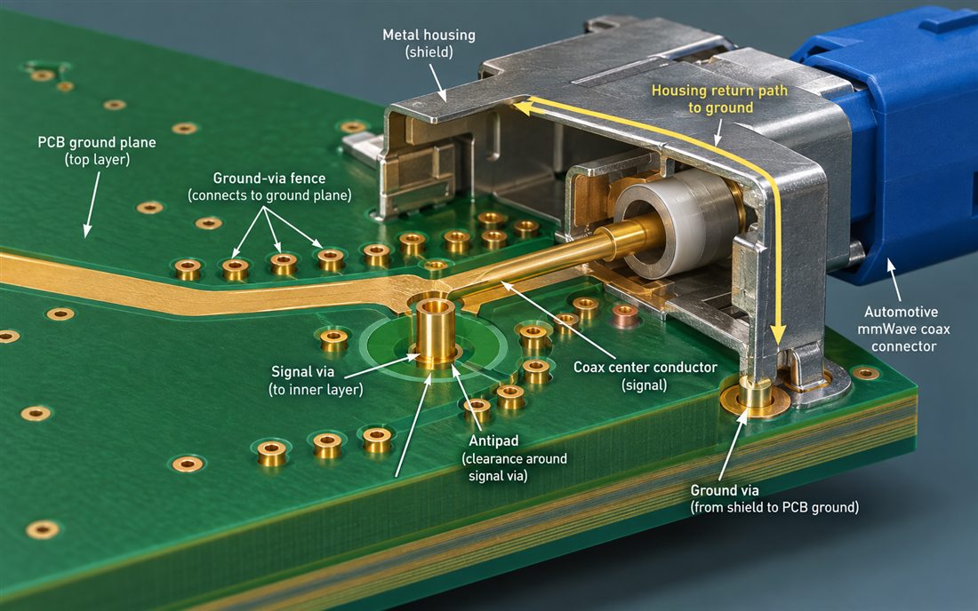
Fix the reference before drawing the footprint. State the board edge or mounting boss used as the mechanical datum, the connector shell or shield reference, the mating height, and the plane that carries the return current. A pin pitch alone is not an electrical specification. For Automotive High Frequency PCB, show the signal layer, the first continuous reference, the connector pad, the antipad, and the path into the cable, antenna, or sensor. The program file should cross-reference multilayer PCB and high-reliability PCB so design and sourcing see the same boundary.
The released Automotive High Frequency PCB page is an internal capability reference; the engineering decision remains in this article and the project file.
Shape the signal and return launch together
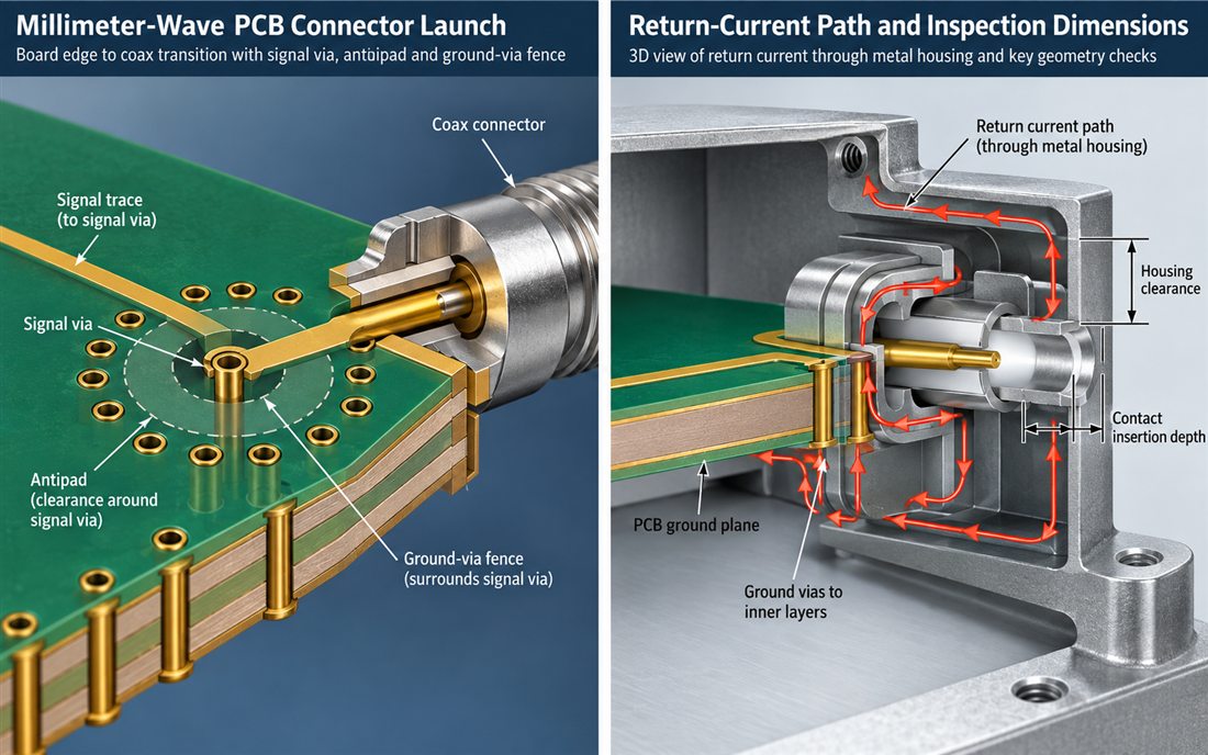
Tune the geometry that fabrication can hold: finished hole, capture-pad diameter, antipad, copper-to-edge clearance, solder-mask opening, and the spacing to the nearest ground via. The PCB layout package should identify which dimensions affect impedance or phase and which are only mechanical. If a flex tail, press-fit terminal, or edge connector is used, add plating thickness and wear limits to the same review rather than leaving them in a separate mechanical note.
The handoff should name RF PCB, thermal management PCB, and via design where those terms describe a controlled physical feature. The released Automotive High Frequency PCB page is an internal capability reference; the engineering decision remains in this article and the project file.
Use fences and planes to control current
A via fence is a current-control feature, not a decorative row of holes. Its pitch, distance from the signal, plane connection, and drill aspect ratio determine how well the return field is contained. Keep the fence continuous through the connector keep-out when the housing allows it, and bridge any plane opening intentionally. The RF PCB design rule should prevent thermal vias, shield gaps, or a random chassis contact from becoming the unintended RF return. Keep surface finish PCB beside the drawing revision and assign turnkey PCB assembly as the verification owner.
The released Automotive High Frequency PCB page is an internal capability reference; the engineering decision remains in this article and the project file.
Define inspection and rework limits
Inspection has to see the same failure modes as the design review. Add cross-section or X-ray checks for critical barrels, annular rings, solder voids, and connector coplanarity; define where rework is allowed; and state how a repaired launch will be reverified. A hot-air repair can lift a pad or change solder volume without leaving an obvious visual defect. The PCB assembly process window should therefore name the rework limit and the post-rework electrical or dimensional check.
The traveller can connect PCB materials with high frequency PCB design and preserve evidence for the next lot. The released Automotive High Frequency PCB page is an internal capability reference; the engineering decision remains in this article and the project file.
Qualify a substitute as a new interface
When a supplier proposes a different connector or terminal, compare pad length, shield geometry, plating, mating height, pin inductance, and strain path. A footprint match is not proof of an electrical match. Require a controlled coupon, a drawing comparison, or a focused pilot before accepting the substitute. This prevents a lead-time decision from moving the antenna phase center or the module’s housing reference without review. Before sign-off, confirm controlled impedance PCB and PCB manufacturing use the same revision and acceptance method.
Release checklist for the next vehicle build
- State the vehicle interface, operating band, and environmental boundary for Automotive High Frequency PCB.
- Identify the controlled material construction, copper profile, and pressed dielectric tolerance.
- Show the signal and return path through connectors, vias, shields, planes, and housing datums.
- Tie fabrication and assembly checks to a revisioned drawing, coupon, or inspection record.
- Label typical values, design targets, engineering ranges, and measured values separately.
- Record the owner and closure evidence for each open RF, thermal, mechanical, and service risk.
Sources: Rogers RO4830 Plus and automotive radar design documents; Analog Devices RF/mixed-signal layout guidance; Qorvo radar application material; and Würth connector signal-integrity application notes. These authoritative engineering references inform the reasoning; no external link is inserted into the article and no customer measurement, certification, or simulation result is implied without retained project evidence.
