
Table of Contents
- Copper profile and loss budget
- Drawing notes and finished geometry
- Cross-section inspection
- Procurement release gate
Taconic RF-35 PCB projects often pass a schematic review and still lose margin at the first production build. The hidden variable is frequently conductor loss: copper roughness, finished trace width, etch shape, and the way the reference plane is built. Treating roughness as a material footnote makes it difficult for an RF designer, buyer, and fabricator to agree on what “low loss” means.
Why Taconic RF-35 PCB copper profile changes a microwave loss budget
At higher frequencies, a Taconic RF-35 PCB carries current concentrated near the conductor surface. A rougher surface increases the effective path length and can raise conductor loss beyond a smooth-copper calculation. The result is not simply a lower insertion-loss number. It can also change phase delay, filter Q, channel-to-channel tracking, and the amount of gain a system must recover in calibration.
A Taconic RF-35 PCB should therefore be released with a declared assumption for copper profile. Public RF-35 data commonly gives a typical Dk around 3.50 and Df around 0.0018 at a specified test frequency. Those values describe the laminate system under a defined method; they do not replace a fabrication note for copper foil, plating, and finished geometry.
| Loss input | Design question | Release evidence |
|---|---|---|
| Copper profile | Is the loss model based on a named foil or a generic smooth conductor? | Foil/plating assumption on stackup |
| Trace geometry | Does finished width include etch and plating bias? | Impedance and cross-section note |
| Reference plane | Are plane roughness and current return treated consistently? | Material and copper callout |
| Frequency band | Does the model cover the highest harmonic of interest? | Frequency sweep or acceptance window |
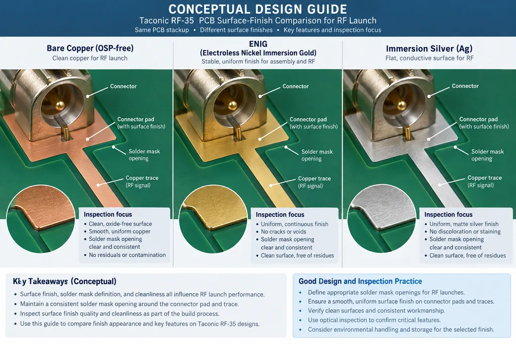
Convert a loss model into a drawing note
Begin with the nets on a Taconic RF-35 PCB that actually consume the loss budget: filter resonators, long feed networks, low-noise receiver paths, and power-amplifier outputs. For each net, record the target impedance, frequency range, trace class, copper weight, and reference layer. A short connector launch may tolerate a different treatment from a long coupled-line filter, but the difference must be intentional.
Specify finished copper rather than only base foil weight when the RF path is sensitive. State whether the trace width is measured before or after plating and whether the solder mask is present in the model. If a design uses a ground-backed coplanar waveguide, include the side-ground copper condition and the via-fence pitch. This makes PCB design intent visible to the CAM and impedance teams.
Do not insert an unverified roughness value on a Taconic RF-35 PCB simply to make a field-solver input complete. If the material supplier or fabricator has not confirmed a number, define a reasonable design range and ask for correlation on the first article. A transparent range is more useful than false precision.
Inspect the finished cross-section, not only the coupon label
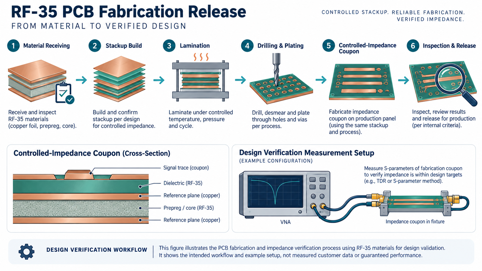
The release team should compare the Taconic RF-35 PCB release the RF trace coupon with the product geometry. Check the finished copper thickness, line width at the top and bottom of the trace, dielectric height to the reference plane, and the presence of resin recession or local voiding. A coupon that uses a different copper weight or a different layer distance cannot prove the product path.
For a Taconic RF-35 PCB, the cross-section review can be tied to a simple loss budget: calculated conductor loss, dielectric loss, connector contribution, and measurement uncertainty. If a measured insertion-loss result falls outside the window, the team can isolate whether the cause is geometry, copper profile, or fixture de-embedding instead of changing the laminate blindly.
Coordinate copper choices with procurement and manufacturing
Copper profile is also a sourcing issue. A buyer may quote a laminate by name while the RF drawing leaves the foil and plating condition open. The result is a nominally correct material with a different conductor-loss behavior. Add the critical copper assumptions to the purchase description and ask for written confirmation of substitutions.
KKPCB’s RF PCB manufacturing review should identify which copper details are standard, which require a special request, and which are verified on a coupon. The same review should check etch compensation, panel orientation, registration, and whether the surface finish is compatible with the connector or probe interface.
Use a release gate that protects RF margin
A practical PCB fabrication gate for a Taconic RF-35 PCB has four questions: Was the copper profile assumption recorded? Does the coupon mirror the critical trace? Is the finished cross-section within the drawing window? Can the test fixture separate board loss from cable and connector loss? A “yes” creates a defensible handoff.
When those questions are closed, a Taconic RF-35 PCB can be evaluated on engineering evidence rather than on a generic low-loss label. That discipline helps project managers protect schedule and budget because a copper-loss escape is found at release, not after an expensive RF retune.
For a complete supplier brief, add a controlled-impedance PCB note and an RF test coupon requirement beside the loss budget.
Sources: public Taconic/AGC RF-35 typical material data; Analog Devices guidance on RF trace geometry, impedance, and return paths; KKPCB manufacturing and inspection workflow information reviewed for this article.
