HomeCategory

PCB Manufacturing Services | High-Quality PCB & PCBA - KKPCB

PCB Material Characterization: Test Methods for High-Frequency and mmWave PCB

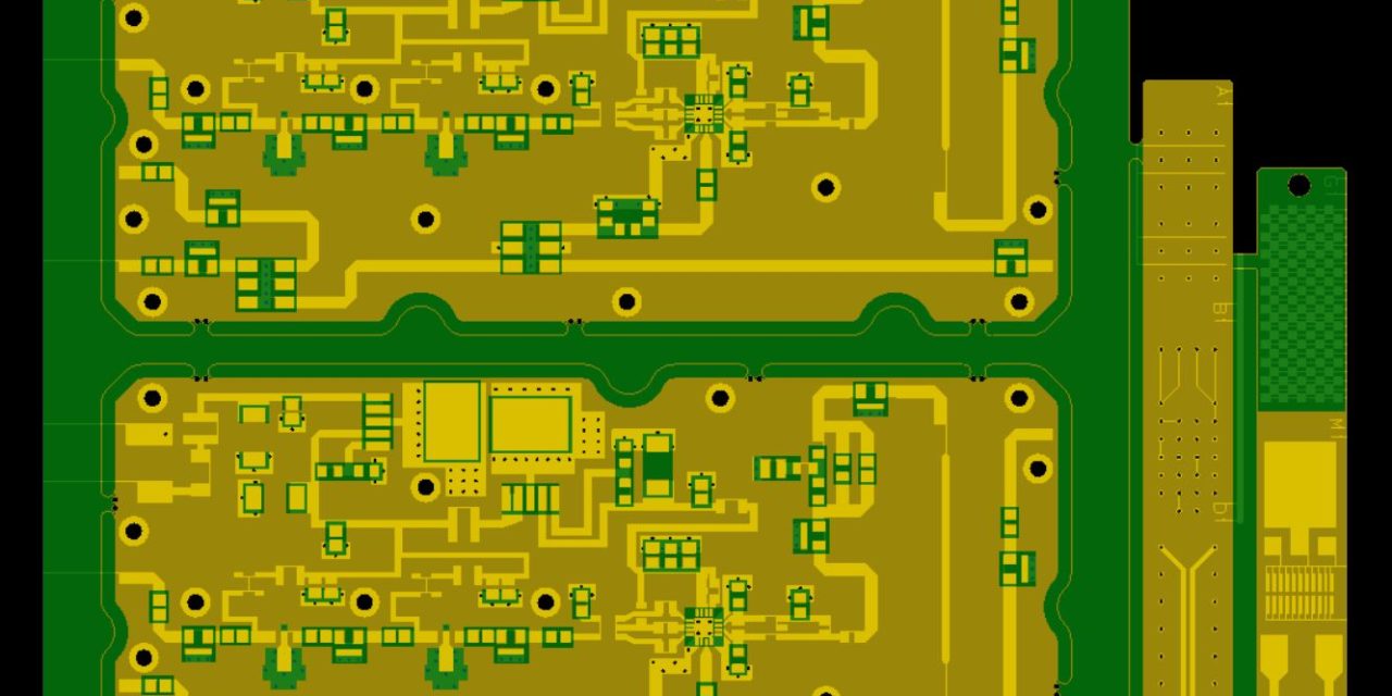
Why PCB Material Characterization Matters at High Frequencies The electrical properties of a PCB material can be characterized using several different measurement techniques. Some methods directly evaluate the dielectric material using specialized fixtures, while others characterize the material through an actual circuit structure. This distinction becomes increasingly important as PCB operating frequencies move from conventional...

High Frequency PCB OEM: End-to-End Manufacturing Solutions for RF and Microwave Applications

As RF, microwave, and high-speed communication technologies continue to evolve, partnering with a reliable high frequency PCB OEM is critical for companies seeking consistent performance, stable quality, and scalable manufacturing. High frequency PCBs operate at GHz and millimeter-wave ranges, where even small variations in materials or processes can significantly impact signal integrity. This article explains...

Rogers RO4003C Laminate: Reliable High-Frequency Material for RF & Microwave PCB Design

Rogers RO4003C: High-Performance Laminate for RF & Microwave PCB Applications Introduction In high-frequency and RF circuit design, material selection directly determines signal quality, thermal stability, and long-term reliability. Among the most trusted high-frequency laminates available today, Rogers RO4003C stands out as a cost-effective, high-performance solution engineered for precision and consistency in demanding RF, microwave, and...

Multilayer PCBs: Balancing Density, Performance, and Scalability

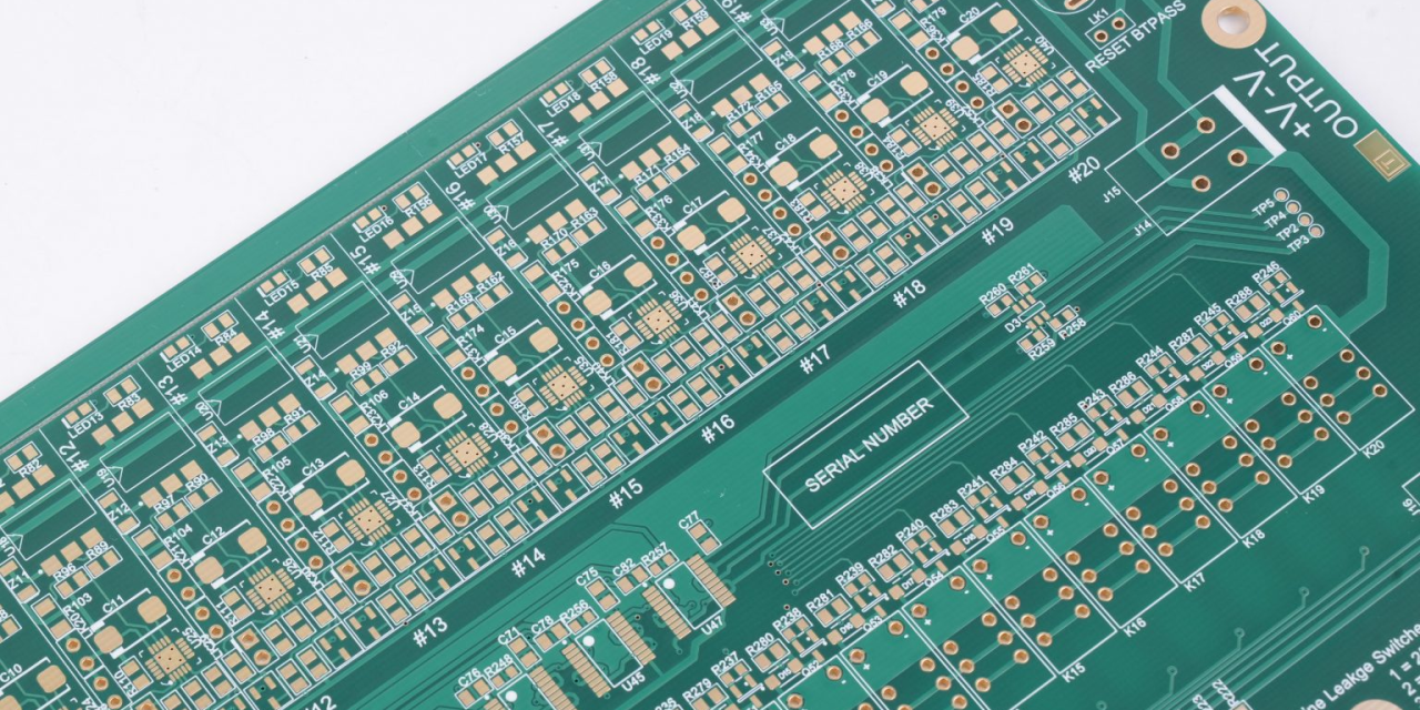
Why Multilayer PCBs Became Standard As electronic systems evolved from simple circuits to highly integrated platforms, single-layer and double-layer PCBs quickly reached their limits. Multilayer PCBs—typically defined as boards with 4 or more layers—became the standard solution for handling increased complexity. By stacking multiple conductive and insulating layers, engineers can: Route more signals within limited...

Blind & Buried Vias in HDI PCB: Design & Manufacturing Expertise

Blind and Buried Vias in HDI PCB Design: Engineering Principles, Manufacturing Constraints, and KKPCB’s Advanced Capabilities As high-density interconnect (HDI) technology becomes essential in 5G, wearables, automotive radar, aerospace, and compact IoT systems, PCB designers increasingly rely on blind vias and buried vias to meet aggressive space, performance, and reliability requirements. These via structures allow...

Phase Stability and High-Temperature Performance Validation of Ceramic PCBs in Automotive Radar and ADAS Sensor Platforms

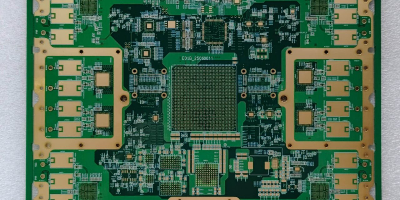
Engineering Context / Abstract Advanced automotive radar and ADAS (Advanced Driver Assistance Systems) platforms demand high-frequency PCB substrates capable of precise phase stability, minimal signal loss, and consistent performance under extreme thermal cycles and vibration. High-density radar modules operating in 77–81 GHz bands are particularly sensitive to dielectric fluctuations, EMI, and thermal expansion, which can...

High Current PCBs: Engineering Reliable Power Delivery for Demanding Applications

What is a High Current PCB? A High Current PCB is a printed circuit board specifically engineered to carry significant electrical current—ranging from several amperes to hundreds of amperes—without excessive heat generation, voltage drop, or reliability issues. Unlike standard PCBs, high current designs must address resistive losses (I²R), thermal buildup, and mechanical stress. If not...