
What is a High Current PCB?
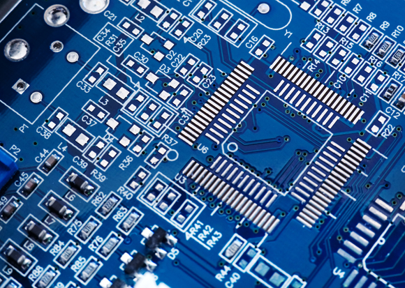
A High Current PCB is a printed circuit board specifically engineered to carry significant electrical current—ranging from several amperes to hundreds of amperes—without excessive heat generation, voltage drop, or reliability issues.
Unlike standard PCBs, high current designs must address resistive losses (I²R), thermal buildup, and mechanical stress. If not properly designed, excessive current can lead to overheating, delamination, or even catastrophic failure.
High current PCBs are commonly used in:
-
Power supply systems and converters
-
Electric vehicles (EVs) and battery management systems
-
Industrial motor drives and automation
-
Renewable energy systems such as solar inverters
High Current PCB Design
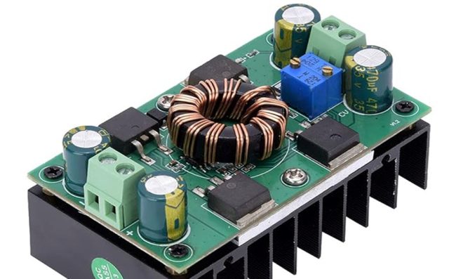
Designing a high current PCB requires a balance between electrical performance, thermal control, and manufacturability:
-
Current Carrying Capacity Calculation:
Engineers calculate trace width based on current, allowable temperature rise, and copper thickness, often referencing IPC-2221 or IPC-2152 standards. Wider traces or copper pours reduce resistance and heat generation. -
Copper Thickness (Heavy Copper Design):
High current PCBs typically use copper weights ranging from 2 oz to 10 oz or more. Heavier copper reduces resistive losses and improves heat dissipation but introduces manufacturing complexity. -
Thermal Management Strategy:
Efficient heat dissipation is critical. Designers use thermal vias, large copper planes, and heat sinks to spread and dissipate heat. In high-power designs, airflow or external cooling may also be required. -
Voltage Drop and Power Distribution:
Uneven current distribution can lead to localized overheating. Proper power plane design and symmetrical routing help ensure uniform current flow and stable voltage levels. -
Component and Connector Considerations:
High current components such as MOSFETs, inductors, and connectors must be rated appropriately. Pads are often reinforced, and multiple vias are used to improve current transfer between layers.
Manufacturing Considerations and QA
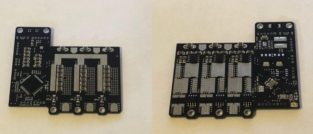
Producing high current PCBs requires specialized fabrication techniques:
-
Heavy Copper Processing: Thick copper layers require controlled etching and plating processes to maintain trace accuracy.
-
Via Reinforcement: Plated through-holes and filled vias ensure reliable interlayer current transfer.
-
Thermal Stress Management: Lamination must accommodate expansion caused by high copper thickness and thermal cycling.
-
Surface Finishes: ENIG or hard gold finishes improve durability and conductivity for high-current contact points.
Quality assurance plays a key role:
-
Thermal Testing: Evaluates temperature rise under load conditions
-
Electrical Testing: Verifies continuity and resistance levels
-
Cross-Section Analysis: Ensures copper thickness and via integrity
-
Reliability Testing: Simulates long-term operation under high current stress
KKPCB applies strict process control and testing standards to ensure high current PCBs operate safely and reliably in demanding environments.
Applications of High Current PCBs
High current PCBs are essential in systems where power delivery is critical:
-
Electric Vehicles (EVs): Battery management systems, motor controllers, and charging modules
-
Industrial Automation: Servo drives, inverters, and heavy machinery control systems
-
Renewable Energy: Solar inverters, wind power converters, and energy storage systems
-
Power Electronics: High-current DC–DC converters and power distribution boards
As power demands continue to increase in modern electronics, high current PCB design becomes increasingly important. With expertise in heavy copper processing, thermal management, and precision manufacturing, KKPCB delivers high current PCB solutions that ensure efficient and reliable power delivery.
