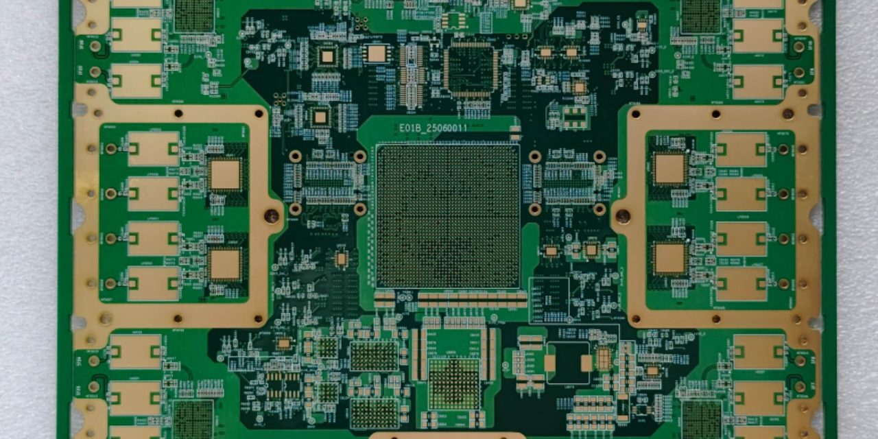
Blind and Buried Vias in HDI PCB Design: Engineering Principles, Manufacturing Constraints, and KKPCB’s Advanc...

Blind and Buried Vias in HDI PCB Design: Engineering Principles, Manufacturing Constraints, and KKPCB’s Advanc...
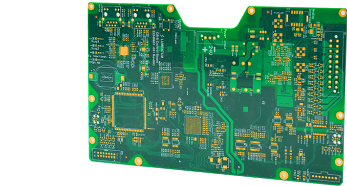
High-Density Interconnect (HDI) PCBs are a key technology for today’s compact and high-performance electronics...
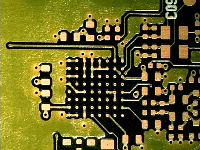
In today’s rapidly evolving electronics market, devices are becoming smaller, faster, and more complex. To mee...
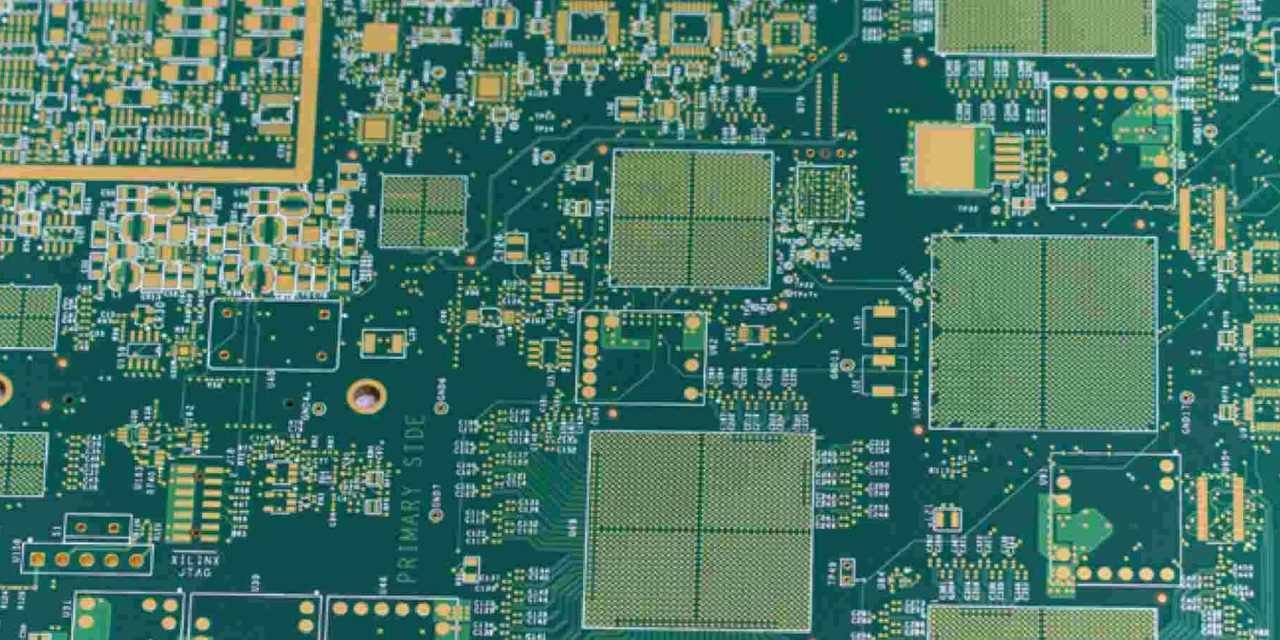
As digital systems move toward higher data rates, smaller form factors, and lower power consumption, the deman...
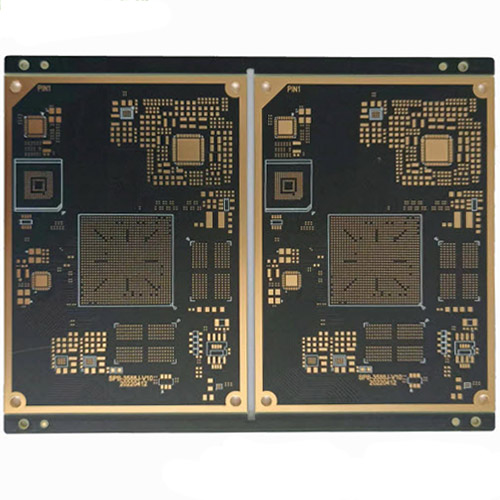
HDI PCB: The Foundation of Modern Electronic Miniaturization In today’s electronics industry, devices are beco...
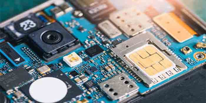
Engineering Context Modern smartphones integrate increasingly complex electronic functions into extremely comp...
KKPCBは、フレックス、リジッドフレックス、RF/マイクロ波、HDI、リジッド多層、およびATEテストボード向けのPCB設計、製造、実装、テストを専門とする大手電子ソリューションプロバイダーです。試作、部品調達、SMT/THT実装、機能テスト、筐体組立、最終製品パッケージングを含む包括的なエンドツーエンドサービスを提供しています。ワンストップの社内体制により、KKPCBはOEMおよびODMソリューションを短納期、高品質、コスト効率よく提供し、世界中の顧客にサービスを展開しています。

PCB製造
PCB実装
技術サポート