HomeCategory

PCB Manufacturing Services | High-Quality PCB & PCBA - KKPCB

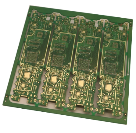
Four Key Points in High-Speed PCB Design

When designing high-speed PCBs, process variations and other factors can significantly impact actual impedance. Automated design tools may not always detect these subtleties, making proactive, defensive design essential. Here’s how to address common challenges in high-speed PCB design. 1. Layer Stack-Up Configuration A well-configured layer stack-up is foundational for signal integrity (SI) and electromagnetic compatibility (EMC). Ideally,...
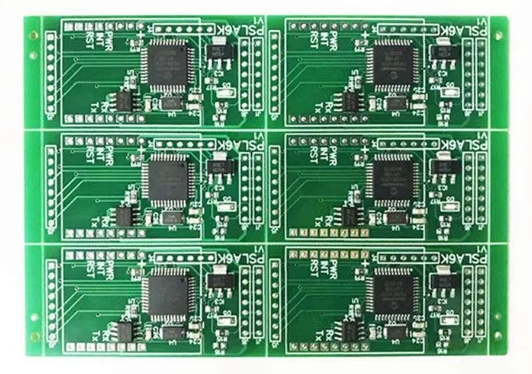
How to Design RF Circuits and PCB Layouts

With the rapid development of wireless communication, radar systems, IoT devices, automotive electronics, and high-speed electronic products, RF (Radio Frequency) circuit design has become increasingly important. Compared with conventional PCB designs, RF PCB design involves more complex challenges related to signal integrity, impedance control, electromagnetic interference (EMI), and material selection. At high frequencies, even small...

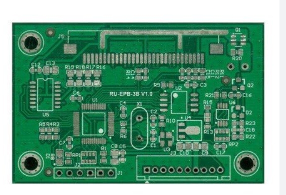
Characteristics of RF Interfaces and RF Circuits in PCB Design

Understanding RF PCB Design in Modern High-Frequency Electronics As wireless communication technology rapidly advances toward: 5G and 6G communication millimeter-wave systems satellite communication automotive radar IoT wireless networks aerospace RF systems the importance of advanced RF PCB design has become increasingly critical. Unlike conventional digital PCB systems, RF circuits in PCB design operate at: high...

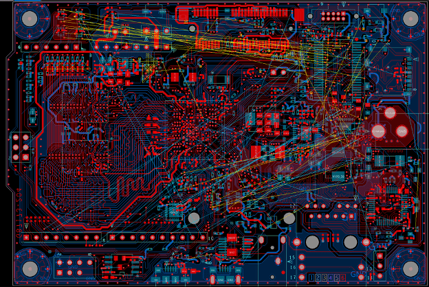
Efficient Automatic PCB Wiring: Skills and Key Points

The rapid evolution of PCB design, with increasingly compact layouts, higher device densities, and stringent performance requirements, has necessitated the adoption of advanced EDA tools. However, achieving high routing efficiency and optimizing the design still requires strategic planning and manual intervention. This guide outlines practical skills and key points for efficient automatic PCB wiring, emphasizing design planning, layout,...

High-Frequency Circuit Design Solution Based on RT/duroid® 6010.2LM Material for Miniaturization

Discover the advantages of RT/duroid® 6010.2LM high-frequency PCB material for compact RF and microwave circuit designs. With a high dielectric constant (Dk 10.7), low loss tangent (0.0026 @10 GHz), excellent thermal stability, and superior mechanical properties, KKPCB helps you achieve miniaturized circuits with high signal integrity for 5G, satellite communications, and high-density PCBs.

High-Speed PCB Copy Board and Design Strategy

With the rapid development of high-speed communication, computing, and advanced electronic systems, PCB designs are required to support increasingly higher data rates while maintaining signal integrity, power stability, and electromagnetic compatibility. At high frequencies, traditional PCB design methods are no longer sufficient. Factors such as impedance variation, signal reflection, crosstalk, dielectric loss, and electromagnetic interference...

The Critical Issue of Near Holes in Multi-Layer PCB Design

In multi-layer PCB design, the primary focus during routing is to ensure efficient and reliable electrical connections between layers using vias. However, as PCB density increases, vias often need to be placed closer together, leading to design and manufacturing challenges. These challenges not only complicate the production process but also impact the long-term reliability of the product....

Experience Sharing in Multi-Layer PCB Impedance Line Routing

With the continuous development of high-speed electronic systems, PCB design is facing increasingly demanding requirements for signal transmission performance. In applications such as communication equipment, industrial control systems, automotive electronics, semiconductor testing equipment, and RF systems, maintaining stable signal quality has become a key factor affecting product reliability. In multilayer PCB design, impedance-controlled routing is...

High-Speed PCB: Optimal Six-Layer Board Structure

When designing high-speed PCBs, the layer stack-up plays a crucial role in ensuring signal integrity, minimizing crosstalk, and achieving optimal electromagnetic compatibility (EMC). For a standard six-layer board with a thickness of 1.6mm, selecting the right structure can significantly impact performance. Below is an analysis of common six-layer board structures and their suitability for high-speed designs....

Basic Knowledge You Need to Master for PCB Design

PCB (Printed Circuit Board) design is a fundamental process in electronic product development. A well-designed PCB not only provides electrical connections between components but also directly affects: Signal integrity Power stability Electromagnetic compatibility (EMC) Thermal performance Manufacturing reliability With the increasing complexity of modern electronic systems, PCB design is no longer limited to simple component...