
With the rapid development of high-speed communication, computing, and advanced electronic systems, PCB designs are required to support increasingly higher data rates while maintaining signal integrity, power stability, and electromagnetic compatibility.
At high frequencies, traditional PCB design methods are no longer sufficient. Factors such as impedance variation, signal reflection, crosstalk, dielectric loss, and electromagnetic interference (EMI) can significantly affect system performance.
A successful high-speed PCB design requires a combination of optimized stackup design, controlled impedance routing, simulation analysis, and manufacturing process control.
High-Speed PCB Design in Different Application Fields
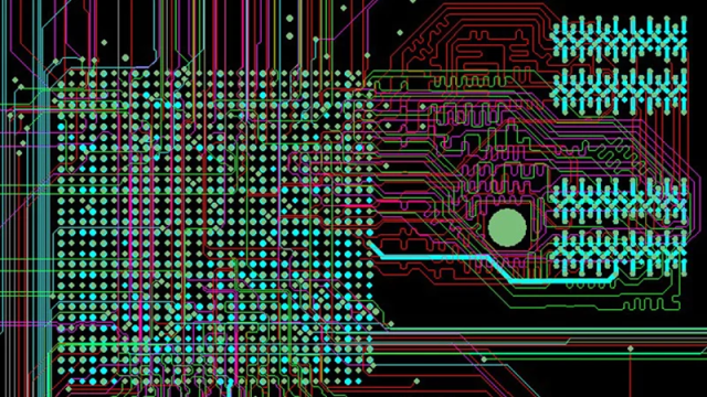
Different industries adopt different design strategies depending on performance requirements, cost limitations, and product lifecycle expectations.
1. High-Speed PCB Design for Telecommunications
Telecommunication equipment typically handles high-volume data transmission, including voice, video, and high-speed network traffic. Data rates can exceed hundreds of Mbps and continue increasing with the evolution of 5G and advanced communication systems.
In this field, PCB performance is usually prioritized over cost optimization.
Key Design Considerations:
High-Layer PCB Structures
Telecommunication PCBs often use complex multilayer structures with dedicated:
- Power layers
- Ground reference layers
- High-speed signal layers
- Shielding structures
These layers help maintain stable power delivery and reduce electromagnetic interference.
Controlled Impedance and Signal Matching
High-speed transmission lines require precise impedance control to minimize:
- Signal reflection
- Insertion loss
- Timing errors
Engineers commonly use impedance simulation and verification methods before manufacturing.
Signal Integrity and EMC Simulation
Before routing, advanced designs typically involve:
- Signal Integrity (SI) simulation
- Power Integrity (PI) analysis
- Electromagnetic Compatibility (EMC) simulation
These simulations help identify potential problems before prototype fabrication.
Performance-Oriented Design Philosophy
Telecommunication products often adopt a performance-first approach, where reliability and time-to-market are more critical than minimizing PCB cost.
2. High-Speed PCB Design for Computer Motherboards
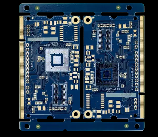
Unlike telecommunications equipment, computer motherboard design requires a balance between performance and cost.
Modern computer systems integrate:
- High-speed CPUs
- DDR memory interfaces
- GPUs
- PCIe interfaces
- High-speed storage devices
These technologies introduce significant signal integrity challenges.
Main Challenges:
Cost Optimization
Many consumer motherboard designs must achieve high performance while maintaining competitive pricing.
This requires engineers to carefully optimize:
- Layer count
- Material selection
- Routing strategy
- Manufacturing cost
High-Speed Interface Management
Critical signals such as:
- DDR memory buses
- PCIe differential pairs
- High-speed clock signals
require precise control of:
- Trace length matching
- Differential impedance
- Crosstalk reduction
- Return current paths
Simulation-Based Optimization
Because cost constraints limit excessive hardware iterations, simulation becomes an important tool for reducing prototype cycles and improving design efficiency.
3. Common Strategies for High-Speed PCB Design
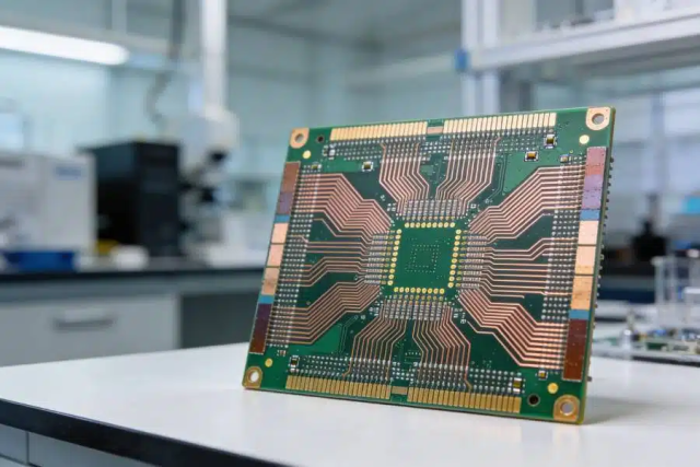
For most electronic products, high-speed PCB design requires a balance between performance, cost, and manufacturability.
Several key strategies are commonly used.
Reference Designs and Manufacturer Guidelines
Many semiconductor manufacturers provide PCB design recommendations for:
- CPUs
- FPGAs
- DSPs
- High-speed interface chips
These guidelines usually include:
- Recommended stackup structures
- Routing constraints
- Impedance requirements
- Power delivery recommendations
However, early reference designs may not cover every application scenario, requiring engineers to optimize based on actual system requirements.
Controlled Design Constraints
Strict design rules help improve reliability by controlling:
- Trace width and spacing
- Differential pair routing
- Length matching
- Via structures
- Layer transitions
However, excessive constraints without proper analysis may increase design complexity and unnecessarily limit layout flexibility.
The best approach is to combine design rules with simulation-based verification.
4. Challenges in High-Speed Signal Matching
Signal termination and impedance matching are common challenges in high-speed PCB design.
For example, a high-speed backplane design may require hundreds of termination components to optimize signal transmission.
Without simulation, engineers may need multiple prototype iterations to adjust resistor values and verify performance.
This approach can result in:
- Longer development cycles
- Increased testing costs
- Additional engineering workload
Using SI simulation tools allows engineers to evaluate different matching strategies before production, reducing trial-and-error optimization.
5. The Importance of Simulation in High-Speed PCB Design
As signal speeds continue increasing, simulation has become an essential part of modern PCB development.
Simulation tools help engineers analyze:
Signal Integrity (SI)
Identify and optimize:
- Signal reflection
- Crosstalk
- Overshoot and undershoot
- Timing errors
Power Integrity (PI)
Evaluate:
- Power plane impedance
- Voltage fluctuations
- Decoupling effectiveness
Electromagnetic Compatibility (EMC)
Predict and reduce:
- EMI radiation
- Noise coupling
- Interference between circuits
Manufacturing Considerations for High-Speed PCBs
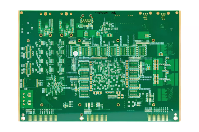
High-speed PCB performance depends not only on design but also on manufacturing accuracy.
Critical manufacturing factors include:
- Stable dielectric thickness
- Controlled Dk/Df material properties
- Precise impedance fabrication
- Low-roughness copper processing
- Accurate layer registration
- Reliable via structures
Even small manufacturing variations can affect high-speed signal performance.
Conclusion
High-speed PCB design requires a comprehensive approach that combines electrical simulation, optimized stackup design, impedance control, and precise manufacturing processes.
Whether applied to telecommunications equipment, computer systems, automotive electronics, or advanced industrial applications, reliable high-speed PCB performance depends on controlling signal integrity from design through production.
At KKPCB, we support high-speed PCB projects with engineering services including stackup optimization, impedance control, SI/EMI considerations, and manufacturing process validation. By integrating engineering expertise with advanced PCB fabrication capabilities, we help customers achieve reliable performance for next-generation high-speed electronic systems.

