
PCB (Printed Circuit Board) design is a fundamental process in electronic product development. A well-designed PCB not only provides electrical connections between components but also directly affects:
- Signal integrity
- Power stability
- Electromagnetic compatibility (EMC)
- Thermal performance
- Manufacturing reliability
With the increasing complexity of modern electronic systems, PCB design is no longer limited to simple component connections. Engineers need to understand circuit principles, material characteristics, layout strategies, manufacturing processes, and reliability requirements.
Whether designing consumer electronics, industrial control systems, communication equipment, or high-frequency circuits, mastering fundamental PCB design knowledge is essential for achieving reliable and manufacturable products.
1. Understanding the Basic Structure of a PCB
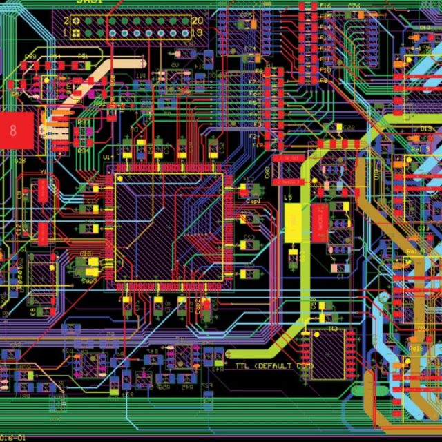
Before starting PCB design, engineers need to understand the basic structure and components of a circuit board.
A typical PCB consists of:
1.1 Copper Layers
Copper layers provide electrical connections.
They can be used as:
- Signal layers
- Power layers
- Ground planes
Multilayer PCBs use multiple copper layers to support complex routing requirements.
1.2 Dielectric Materials
The dielectric layer separates copper layers electrically.
Common materials include:
- FR-4
- High-Tg FR-4
- Rogers laminates
- PTFE materials
- Ceramic substrates
Material selection affects:
- Impedance
- Signal loss
- Thermal performance
1.3 Solder Mask
The solder mask protects copper traces and prevents solder bridging during assembly.
Functions include:
- Insulation protection
- Corrosion prevention
- Improved assembly reliability
1.4 Surface Finish
Surface finish protects exposed copper pads.
Common options include:
- ENIG
- HASL
- Immersion silver
- OSP
Selection depends on:
- Component type
- Assembly process
- Reliability requirements
2. Basic Circuit Knowledge
PCB design is closely connected with circuit theory.
Engineers should understand:
2.1 Voltage, Current, and Resistance
Basic electrical relationships determine:
- Trace width selection
- Power distribution
- Component ratings
Understanding current flow helps avoid:
- Overheating
- Voltage drops
- Circuit failures
2.2 Analog and Digital Circuits
Different circuits require different PCB design strategies.
Analog Circuits
Sensitive to:
- Noise
- Ground interference
- Signal distortion
Examples:
- Amplifiers
- Sensor circuits
Digital Circuits
Require attention to:
- Signal timing
- Clock routing
- High-speed transmission
Examples:
- Microcontrollers
- Processors
2.3 Power Supply Circuits
Power circuits require special attention to:
- Current capacity
- Thermal management
- Voltage stability
Important design factors include:
- Trace width
- Copper thickness
- Grounding structure
3. PCB Schematic Design Knowledge
The schematic is the foundation of PCB layout.
Engineers should understand:
3.1 Component Symbols and Libraries
Correct component libraries ensure:
- Accurate footprints
- Proper assembly
- Reduced design errors
3.2 Netlist Management
The netlist defines electrical connections between components.
Proper netlist management prevents:
- Incorrect connections
- Missing signals
- Layout mistakes
3.3 Design Rule Checking (DRC)
DRC verifies whether the design follows manufacturing requirements.
Checks include:
- Trace spacing
- Hole size
- Clearance rules
- Layer constraints
4. PCB Layout Fundamentals
4.1 Component Placement Principles
Good component placement improves:
- Electrical performance
- Assembly efficiency
- Thermal distribution
Basic principles:
- Place critical components first
- Keep related components close
- Separate noisy and sensitive circuits
4.2 Signal Flow Planning
PCB layout should follow the functional signal path.
A typical design flow:
Input → Processing → Output
This reduces:
- Unnecessary routing
- Signal interference
4.3 Keep Critical Signals Short
Sensitive signals include:
- Clock signals
- RF signals
- High-speed data lines
Short routing helps reduce:
- Signal loss
- Crosstalk
- Timing issues
5. PCB Stack-Up Design Knowledge
For multilayer PCBs, stack-up design is critical.
Engineers need to understand:
5.1 Layer Arrangement
Typical layer functions:
- Signal layers
- Ground planes
- Power planes
Proper arrangement improves:
- Signal integrity
- EMI performance
5.2 Controlled Impedance
High-speed circuits require accurate impedance control.
Factors affecting impedance:
- Trace width
- Copper thickness
- Dielectric thickness
- Material dielectric constant
Common requirements:
- 50Ω single-ended
- 90Ω/100Ω differential
5.3 Balanced Stack-Up Design
A balanced stack-up helps reduce:
- PCB warpage
- Mechanical stress
- Manufacturing variation
Important considerations:
- Symmetrical layer structure
- Balanced copper distribution
6. PCB Wiring Knowledge
6.1 Trace Width and Spacing
Trace dimensions affect:
- Current carrying capability
- Signal quality
- Manufacturing reliability
Higher current requires:
- Wider traces
- Larger copper areas
6.2 Via Design
Vias connect different PCB layers.
Common types:
- Through vias
- Blind vias
- Buried vias
- Microvias
Via design affects:
- Routing density
- Signal performance
- Manufacturing cost
6.3 Differential Pair Routing
Used in:
- USB
- Ethernet
- PCIe
- LVDS
Important rules:
- Maintain spacing consistency
- Match trace lengths
- Keep reference planes continuous
7. Signal Integrity Knowledge
Modern PCB designers must understand signal integrity.
Key issues include:
7.1 Crosstalk
Caused by:
- Parallel trace coupling
- Insufficient spacing
Solutions:
- Increase spacing
- Add ground shielding
- Optimize routing direction
7.2 Signal Reflection
Caused by:
- Impedance mismatch
- Long transmission lines
Solutions:
- Controlled impedance design
- Proper termination methods
7.3 Electromagnetic Interference (EMI)
Poor PCB design can increase radiation.
Solutions include:
- Proper grounding
- Short return paths
- Shielding structures
8. Power Integrity Design Knowledge
Power integrity ensures stable power delivery.
Important factors:
8.1 Power Plane Design
Benefits:
- Lower impedance
- Better current distribution
- Reduced noise
8.2 Decoupling Capacitor Placement
Decoupling capacitors should be:
- Close to IC power pins
- Connected with short traces
This reduces:
- Voltage fluctuations
- High-frequency noise
8.3 Grounding Methods
Proper grounding is essential.
Common approaches:
- Ground planes
- Star grounding
- Digital/analog ground separation
9. Thermal Management Knowledge
Heat management directly affects PCB reliability.
Engineers should consider:
9.1 Heat Sources
Common heat-generating components:
- Power ICs
- MOSFETs
- Regulators
- LEDs
9.2 Thermal Vias
Thermal vias help transfer heat between layers.
Applications:
- Power devices
- High-current circuits
9.3 Copper Area Optimization
Large copper areas improve:
- Heat spreading
- Current handling capability
10. PCB Manufacturing Knowledge
A good PCB design must consider manufacturing capability.
Important manufacturing factors include:
10.1 DFM (Design for Manufacturing)
DFM review evaluates:
- Trace width
- Spacing
- Via structures
- Assembly requirements
10.2 SMT and THT Assembly Requirements
Designers should consider:
- Component placement
- Soldering process
- Inspection requirements
10.3 Testing Requirements
PCB design should support:
- ICT testing
- Functional testing
- AOI inspection
Proper test design improves production efficiency.
11. Common PCB Design Mistake
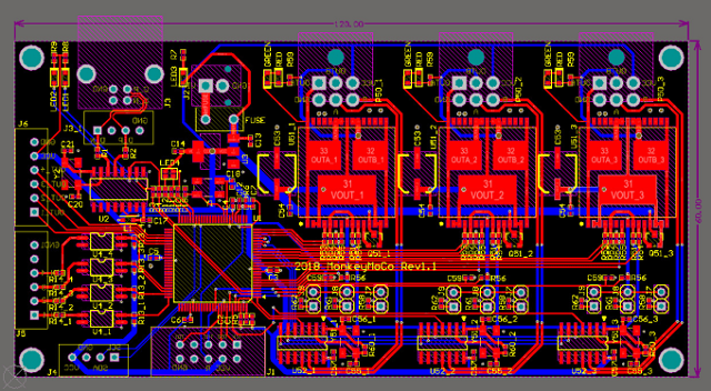
Ignoring Manufacturing Capability
Problem:
Design exceeds fabrication limitations.
Result:
- Increased cost
- Lower yield
Poor Ground Design
Problem:
Unstable return paths.
Result:
- Noise
- EMI problems
Incorrect Component Placement
Problem:
Poor functional organization.
Result:
- Difficult routing
- Performance issues
Lack of Thermal Planning
Problem:
Heat accumulation.
Result:
- Reduced reliability
12. Recommended PCB Design Workflow
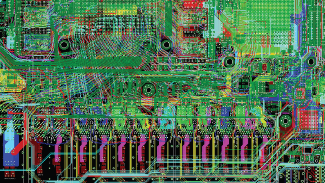
Step 1: Understand Requirements
Analyze:
- Circuit functions
- Operating environment
- Performance requirements
Step 2: Complete Schematic Design
Confirm:
- Component selection
- Electrical connections
Step 3: Plan PCB Stack-Up
Define:
- Layer count
- Materials
- Impedance requirements
Step 4: Component Placement
Prioritize:
- Main ICs
- Power components
- Critical interfaces
Step 5: Routing and Optimization
Complete:
- Signal routing
- Power routing
- Ground design
Step 6: Verification
Perform:
- DRC checking
- Signal analysis
- DFM review
Conclusion
PCB design requires a combination of electrical knowledge, layout skills, manufacturing understanding, and reliability considerations.
The essential knowledge areas include:
- Circuit fundamentals
- Component selection
- PCB structure
- Stack-up design
- Routing techniques
- Signal integrity
- Power integrity
- Thermal management
- Manufacturing requirements
By mastering these fundamentals, engineers can create PCB designs that achieve better performance, higher reliability, and smoother transition from prototype to mass production.

