HomeTag

PCB manufacturing - KKPCB

TLY-5 PCB for Ku-Band Front Ends: Managing Copper Roughness and Phase Repeatability

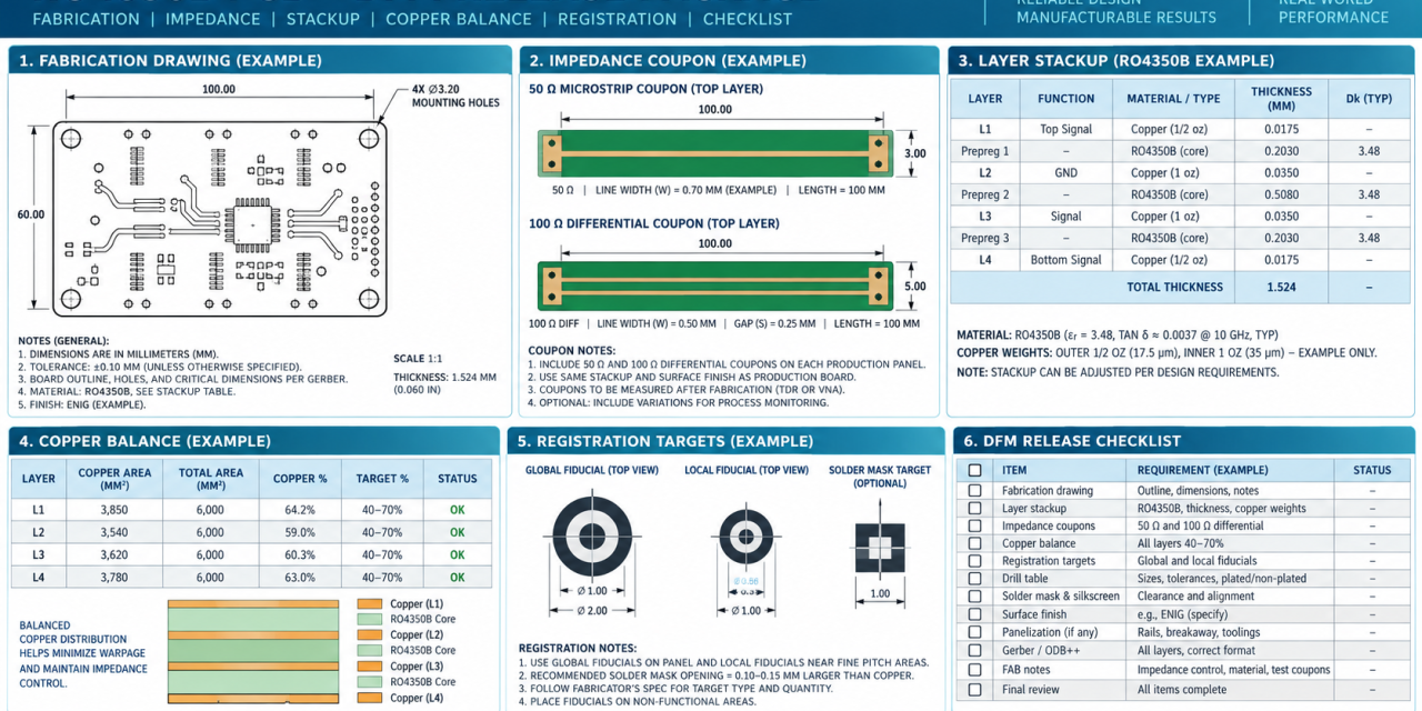
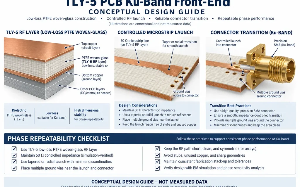
Ku-band TLY-5 PCB projects need a finished-board reference, not only a laminate name. Table of Contents Finished-board sensitivity Copper roughness Connector launch Phase repeatability Manufacturing handoff Release checklist TLY-5 PCB is often selected for a Ku-band front end because the laminate combines a low nominal dielectric constant with low dielectric loss. The difficult part is...
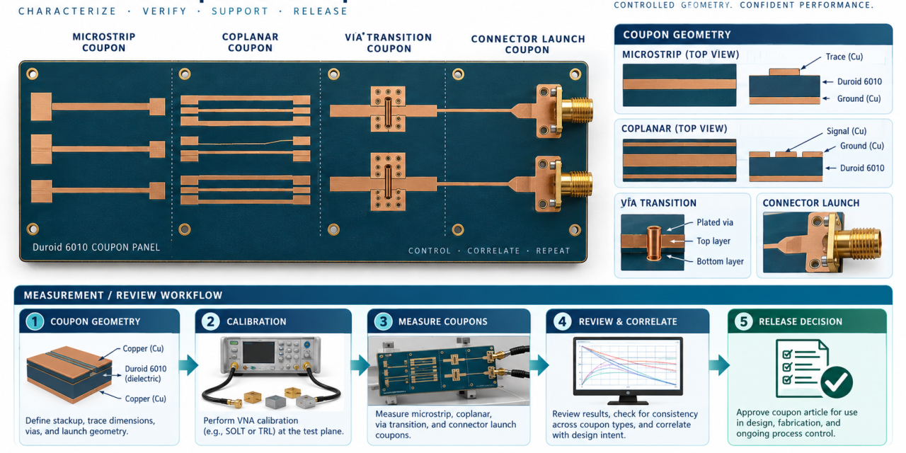
Duroid 6010 PCB Impedance Coupons: 7 Critical Controls for Production Release

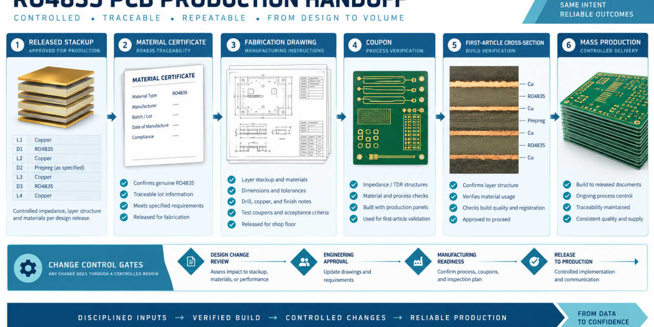
Table of Contents Why coupon design must follow the RF path Seven controls for defensible coupon evidence Geometry, calibration, and correlation Release package and handoff Coupon checklist A Duroid 6010 PCB impedance coupon is useful only when its geometry, construction, fixture, and acceptance method represent the product feature being released. The project pain point is...

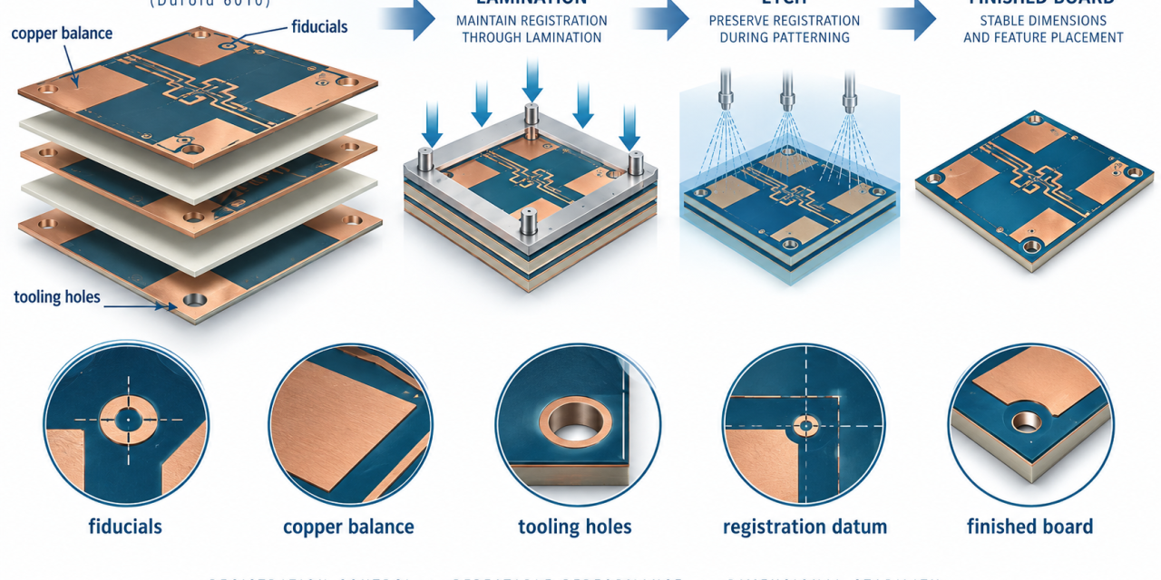
Duroid 6010 PCB Dimensional Stability: 7 Critical Controls for RF Registration

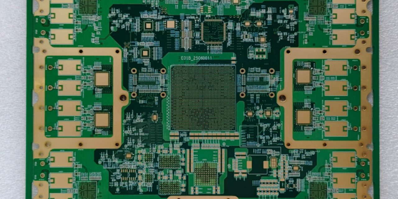
Table of Contents Why dimensional drift affects RF builds Seven controls for registration stability Panel balance and datums Inspection and release evidence Project checklist A Duroid 6010 PCB can be electrically well designed and still miss the project’s RF margin when layer-to-layer registration, copper balance, or board-edge datums drift through lamination and etch. The real...

RO4350B PCB RF Edge Launch: Surface Finish and Connector Reliability

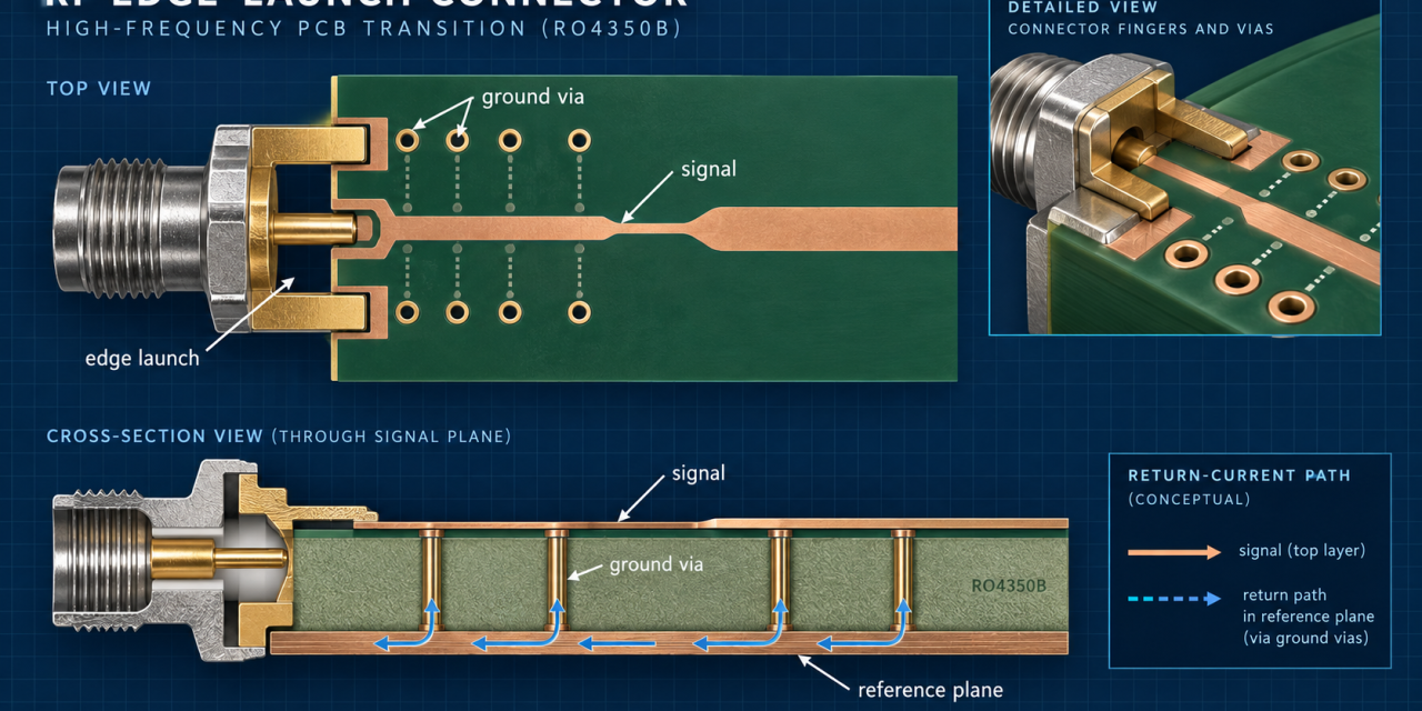
RF edge launches are often tuned electrically and then weakened by a small production detail: an uncontrolled surface finish, a connector land that changes during etch, or a ground transition that does not meet the enclosure. This guide uses the RO4350B PCB to organize an edge-launch review around electrical intent, finish selection, and repeatable inspection....

Blind & Buried Vias in HDI PCB: Design & Manufacturing Expertise

Blind and Buried Vias in HDI PCB Design: Engineering Principles, Manufacturing Constraints, and KKPCB’s Advanced Capabilities As high-density interconnect (HDI) technology becomes essential in 5G, wearables, automotive radar, aerospace, and compact IoT systems, PCB designers increasingly rely on blind vias and buried vias to meet aggressive space, performance, and reliability requirements. These via structures allow...

PCB Quotation Request: Key Information Required for Accurate PCB Manufacturing Pricing

Why a Complete PCB Quotation Request Matters In the PCB manufacturing industry, an accurate PCB quotation request is essential for: Faster engineering evaluation Accurate production pricing Reduced communication delays Shorter project lead times Better manufacturing feasibility analysis Whether the project involves: Standard multilayer PCB High-frequency RF PCB HDI PCB Flexible PCB PCB assembly (PCBA) a...

Fine Line PCBs: Pushing the Limits of Precision and Density in Modern Electronics

What Is a Fine Line PCB? A Fine Line PCB refers to a board manufactured with extremely narrow trace width and spacing, typically: ≤100 µm (4 mil) → standard fine line ≤75 µm (3 mil) → advanced ≤50 µm (2 mil) or below → ultra-fine line These geometries go beyond conventional PCB fabrication limits and...

Multilayer PCB: Advanced Design for High-Density and High-Speed Electronics

Multilayer PCB: Advanced Design for High-Density and High-Speed Electronics With modern electronic devices becoming increasingly compact and high-performance, Multilayer PCB technology is essential for achieving complex circuit routing, improved signal integrity, and efficient power distribution. A multilayer PCB consists of three or more conductive copper layers laminated together with dielectric materials , enabling compact, high-density,...