
RF edge launches are often tuned electrically and then weakened by a small production detail: an uncontrolled surface finish, a connector land that changes during etch, or a ground transition that does not meet the enclosure. This guide uses the RO4350B PCB to organize an edge-launch review around electrical intent, finish selection, and repeatable inspection. The figures are engineering illustrations, not customer test photographs.
Start with the connector and board-edge datum
The RO4350B PCB launch should define the connector land, board edge, reference plane, copper treatment, and finished dielectric in one controlled drawing. If the mechanical datum moves, the RF taper and ground-via fence move with it. Freeze the connector footprint before the stackup is sent for quotation.
| Release item | Production risk | Control |
|---|---|---|
| Edge datum | Connector misalignment | Dimension from a controlled mechanical feature |
| Surface finish | Contact or solder variation | Specify approved finish and inspection method |
| Launch taper | Local impedance step | Review after etch compensation |
| Ground stitching | Return-current detour | Keep vias inside the released launch envelope |
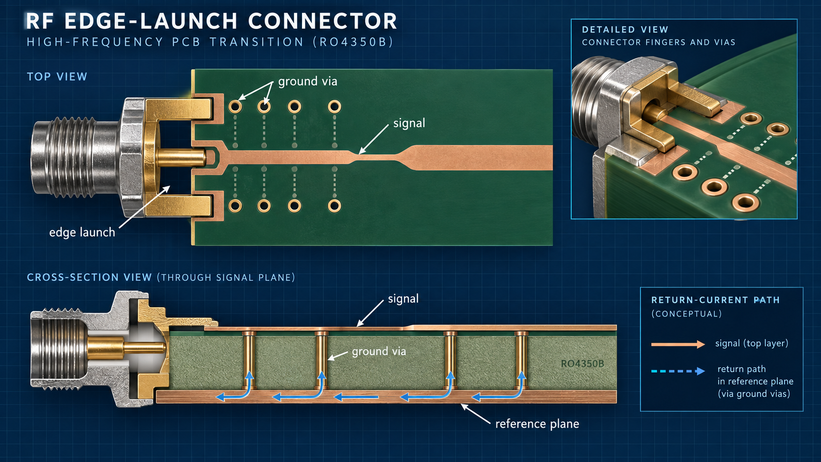
Illustrative RF edge-launch cross-section with connector fingers, ground stitching vias, and reference plane.
Choose finish requirements around the interface
Surface finish is a system choice. A connector contact, soldered RF shield, and fine-pitch assembly pad may need different acceptance language. For a controlled impedance PCB, the finish note must not change the finished copper or launch geometry without an engineering review. Use supplier-typical information as design context, then verify the released process with the fabricator.
Questions for the edge-launch review
- Is the selected finish compatible with the connector contact and assembly flow?
- Are solder-mask openings and edge clearances defined after manufacturing compensation?
- Does the launch keep a continuous reference under the signal path?
- Are contact wear, contamination, and handling controls assigned to an owner?
- Is the acceptance method documented without implying an unperformed test?
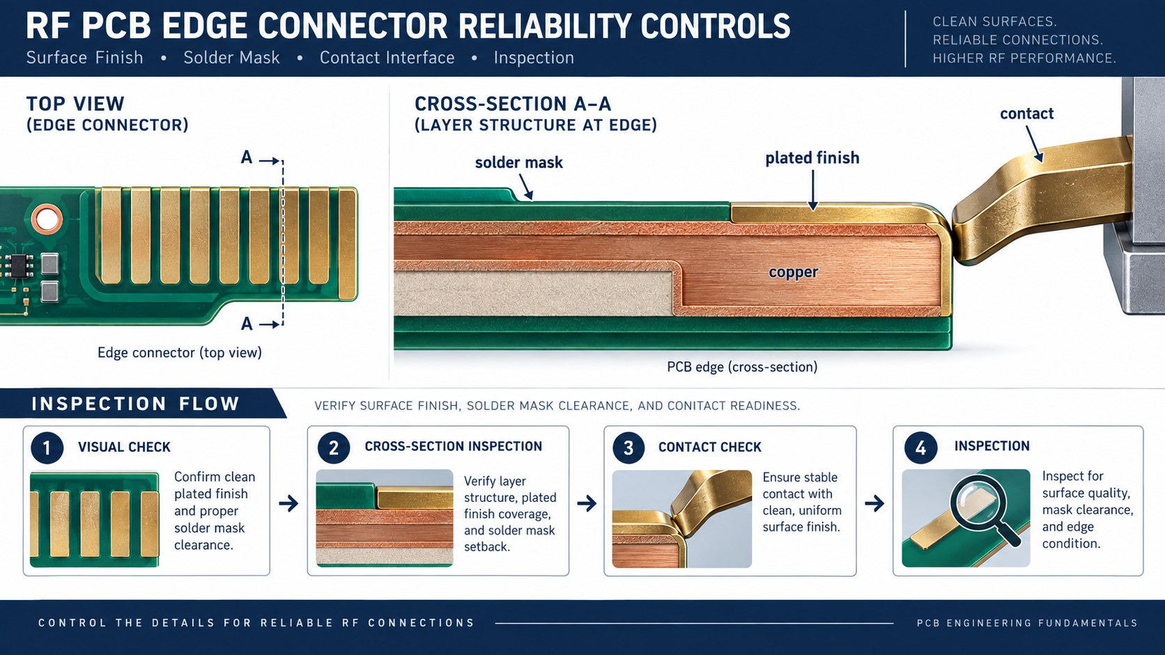
Illustrative surface-finish inspection concept showing copper, plated finish, solder mask, and contact areas.
Protect the return path at the board edge
The multilayer PCB stackup should reserve a low-inductance ground route near the connector. Place stitching vias with enough clearance for drilling and plating, and check the edge profile against the enclosure datum. If the design uses an HDI PCB escape, keep microvia and sequential-lamination notes on the same release.
- Compare the connector footprint with the mechanical model.
- Check the RF neck-down after etch compensation and mask definition.
- Keep ground vias clear of the connector body and board edge.
- Document any controlled-depth or backdrill feature near the launch.
- Route every deviation through an ECO with a named approver.
Example inspection and handoff gates
In an illustrative project, the RO4350B PCB handoff can require drawing-to-CAD comparison, edge-profile inspection, finish verification, and a representative coupon plan before volume release. The PCB manufacturing traveler should separate target values from measured evidence and identify the fixture, sample size, and environmental conditions for any test report.
Questions from RF and sourcing teams
Can a finish change be treated as cosmetic?
No. It can affect contact behavior, solderability, copper dimensions, and the assumptions used in the launch model.
Does a connector ground shell replace stitching vias?
Not automatically. The shell, board vias, reference plane, and enclosure interface must be reviewed as one return-current path.
What must be frozen before release?
Freeze the edge datum, connector land, finish specification, launch geometry, stackup, inspection method, and deviation authority.
Sources: Vendor-typical RO4350B material context and KKPCB public High-Frequency PCB, PCB Materials, Multilayer PCB, HDI PCB, and PCB Manufacturing categories. No external hyperlinks or claimed customer measurements are used.
For the final RO4350B PCB release, keep the RO4350B PCB connector drawing, finish note, return-path geometry, and inspection record under one controlled revision.
At final review, compare the RO4350B PCB launch drawing with the RO4350B PCB traveler and record the approved finish, edge datum, inspection sample, and deviation owner before release.
