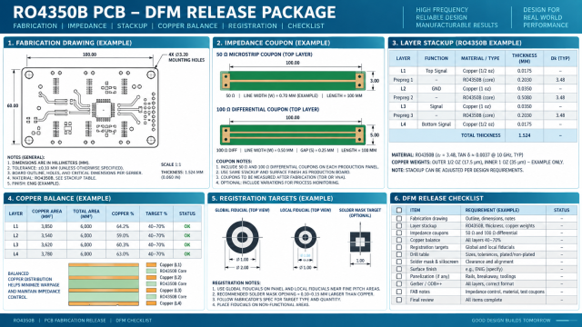
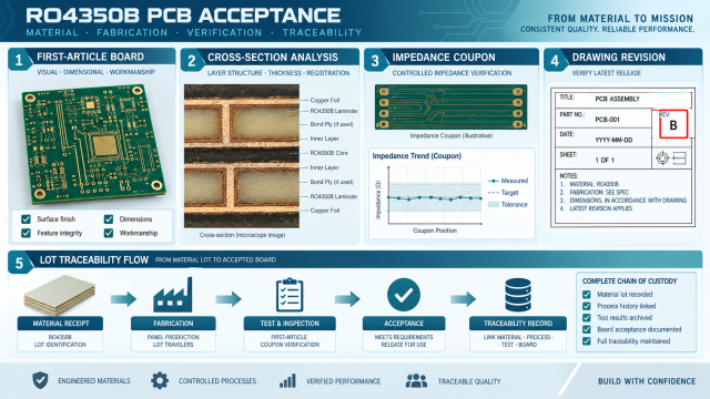
Production acceptance is where a promising RF design becomes a repeatable product. This guide uses the RO4350B PCB as the example for a DFM release that protects impedance, copper geometry, and traceability without claiming customer test results. Values are planning guidance and must be confirmed against the released drawing.
Why RF acceptance fails after the design review
A design team can approve a nominal stackup and still receive panels with a different finished dielectric, copper profile, or solder-mask registration. The RO4350B PCB acceptance package therefore needs a controlled material callout, revisioned stackup, and clear ownership for deviations.
| Release item | Risk if omitted | Acceptance action |
|---|---|---|
| Material and lot | Unapproved laminate substitution | Match approved source and revision |
| Finished dielectric | Impedance drift | Verify construction before panel release |
| Copper profile | Etch and loss variation | Record copper class and treatment |
| Coupon plan | No evidence for process shift | Define coupon type and owner |
Turn impedance intent into a fabricator checklist
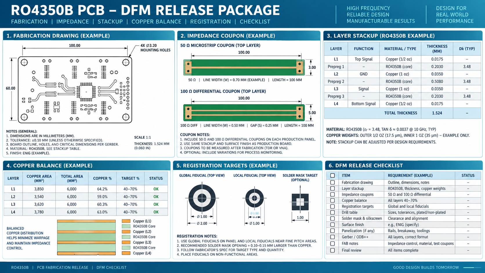
For a controlled impedance PCB, specify the target line, reference layer, finished dielectric assumption, copper thickness, and tolerance method. Do not mix a field-solver target with a coupon measurement as if they were the same evidence. The stackup owner should sign the final construction before the PCB manufacturing traveler is released.
Coupon and traceability controls
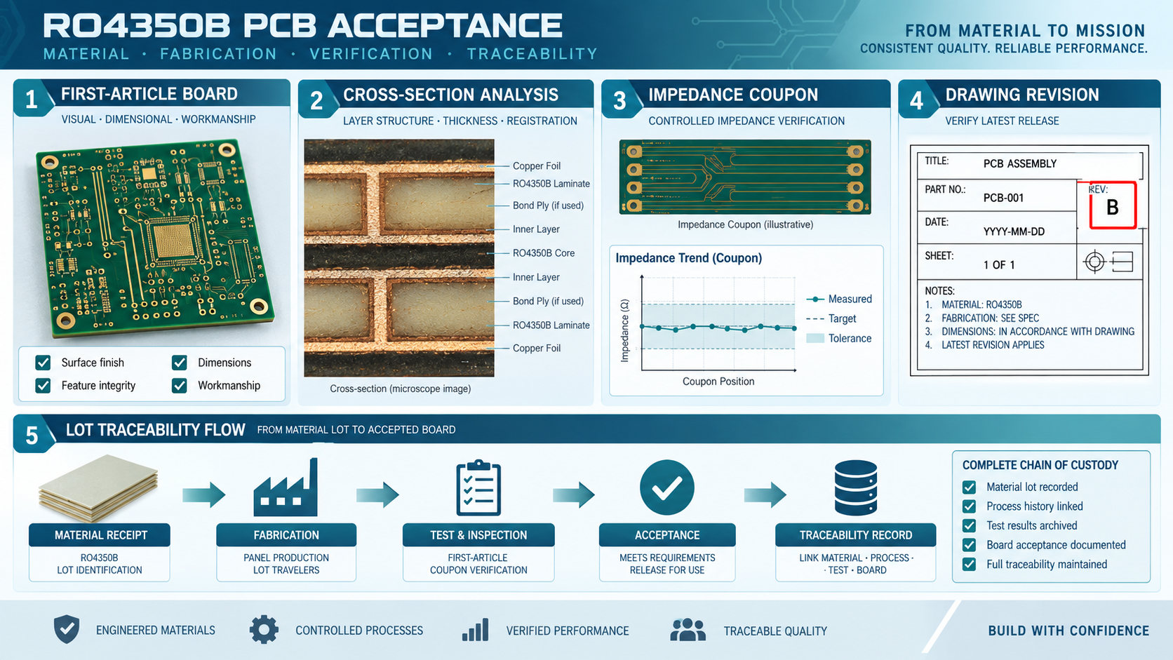
Use a coupon that represents the critical RF geometry and place it where the panel process sees similar plating and etch conditions. Record panel number, laminate lot, press cycle, and measurement method. If the coupon is not representative, label it as a process monitor rather than a direct line-performance proof.
DFM checks that prevent avoidable rework
The multilayer PCB review should check copper balance, drill-to-copper clearance, backdrill depth, solder-mask openings, and edge features. RF launches should keep their return path continuous, while thermal pads must remain compatible with the selected via and plating process.
- Confirm annular ring and registration rules against the released drill class.
- Check RF neck-downs after etch compensation, not only in CAD.
- Keep copper pours balanced so panel bow and twist remain manageable.
- Define controlled-depth routing and backdrill notes on the fabrication drawing.
- Link every deviation to an ECO and an owner before shipment.
Acceptance gates for engineering and purchasing
A purchasing team needs a concise gate sheet, not an informal promise. The RO4350B PCB order should reference the released Gerbers, drill files, stackup, impedance notes, inspection plan, and approved deviation path. If an HDI PCB escape is present, add microvia reliability and fill requirements to the same review.
Design targets versus measured evidence
Target impedance, insertion loss, thermal limits, and dimensional tolerances belong in the design specification. Measured values belong in a report with fixture, calibration, sample size, and environmental conditions. KKPCB capability statements are not a substitute for a project-specific test report.
Questions project managers ask
Can a nominal Dk approve a material change?
No. Recheck finished thickness, copper treatment, resin behavior, and the complete RF path.
Is one coupon enough for every variant?
Only when the variant shares the same critical geometry and process exposure; otherwise define a representative coupon for each family.
What should purchasing freeze first?
Freeze the material system, stackup revision, acceptance method, and deviation authority before negotiating volume.
Sources: Vendor-typical RO4350B material context and KKPCB public High-Frequency PCB, PCB Materials, Multilayer PCB, HDI PCB, and PCB Manufacturing categories. No external hyperlinks or claimed customer measurements are used.
Final release rule
The RO4350B PCB package is ready when its material callout, impedance intent, DFM limits, coupon method, and inspection ownership share one revision. Keep the RO4350B PCB traveler aligned with the engineering release so production acceptance remains auditable.
Keep the RO4350B PCB stackup, RO4350B PCB coupon, RO4350B PCB inspection plan, and RO4350B PCB deviation record on the same checklist.