Blog

Explore the KKPCB Blog for the latest PCB manufacturing and assembly news, industry insights, expert tips, and technology trends, helping you stay informed and optimize your electronics projects.
Aluminum Nitride PCB Direct-Bond Copper: Metallization and Via Reliability Before Qualification

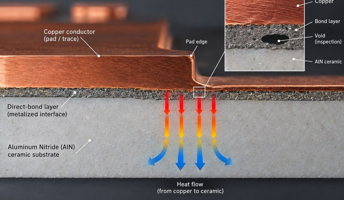
An Aluminum Nitride PCB direct-bond copper release needs a controlled metallization edge, via transition, and inspection record before qualification. Direct-bond copper can deliver a low-resistance thermal and electrical interface on aluminum nitride, but its edge, adhesion, and transition features must survive the same thermal history as the product. A qualification coupon that omits the heavy...
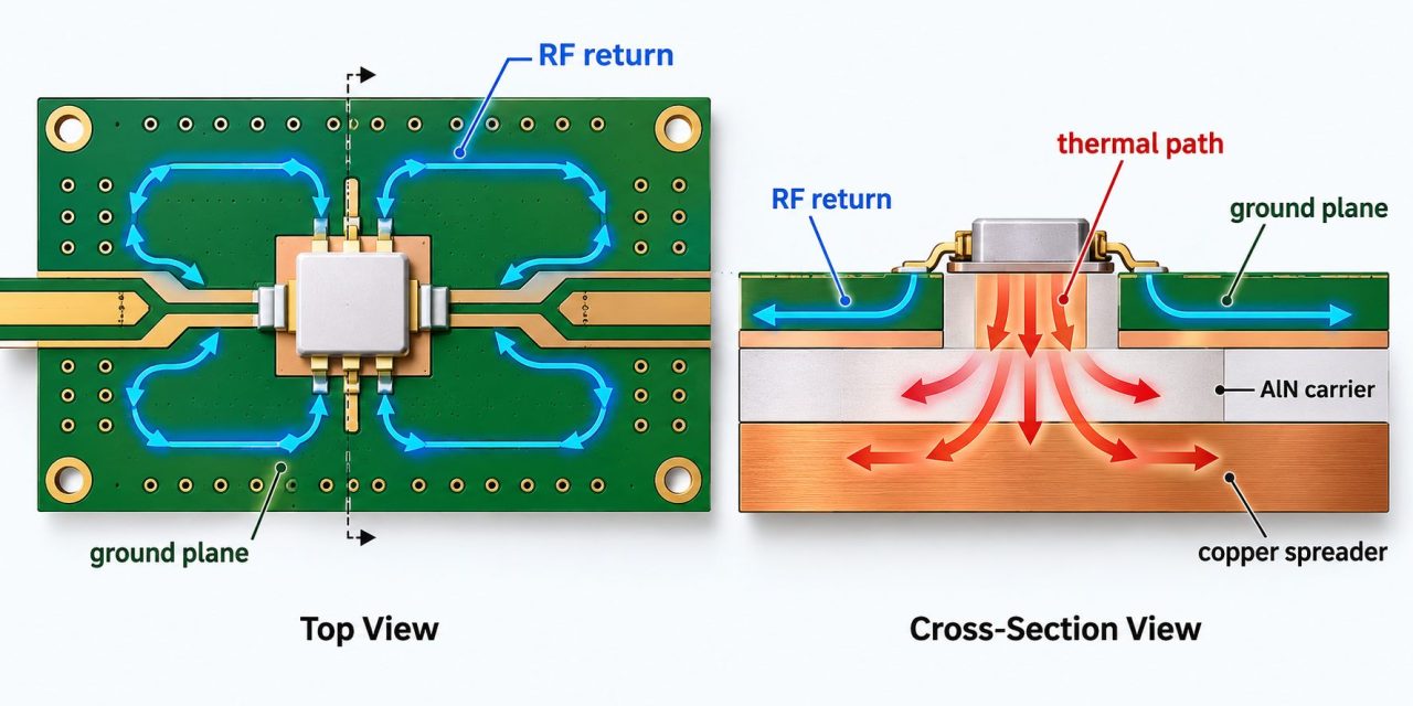
Aluminum Nitride PCB RF Power Layout: Separating Return Current from Heat Spreading

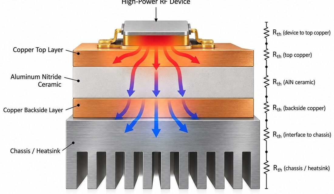
An Aluminum Nitride PCB power layout must release current return and heat through the same controlled interface before the module is approved. RF power boards built on aluminum nitride combine a low-loss electrical path with a high-conductivity thermal path, but the two paths do not always want the same copper geometry. A power island may...

Aluminum Nitride PCB Thermal Paths for RF Power: Releasing Copper and Carrier Interfaces

A power amplifier module can have a favorable ceramic thermal value and still miss its temperature margin because the heat path is not released as a complete assembly. An Aluminum Nitride PCB shares heat and RF functions with copper, solder or braze, a carrier, and the enclosure. The project pain is usually an interface assumption:...

Alumina PCB DFM: Metallization, Panel Handling, and Inspection Before Volume Release

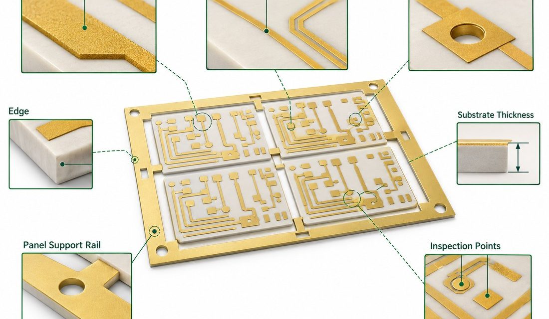
Volume release exposes the difference between a ceramic layout and a ceramic process. Screen, thick-film, thin-film, plated, brazed, and bonded features each have a different capability window. An Alumina PCB drawing that specifies only line widths and hole sizes can still leave the supplier guessing about paste, firing, edge handling, carrier support, and inspection. The...

Alumina PCB for Automotive Sensors: Moisture, Vibration, and Connector Edge Decisions

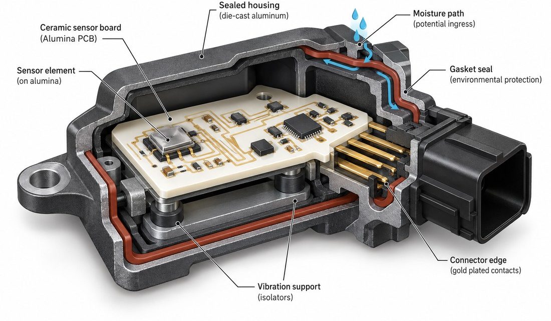
Automotive sensor modules combine a ceramic substrate with a connector, housing, adhesive, shield, and sometimes a high-frequency antenna. The Alumina PCB is stable, but the assembled module still sees vibration, thermal cycling, condensation, and connector loads. The project pain is often a fracture or intermittent contact at an edge feature that was reviewed only as...

Alumina PCB High-Power Reliability: Thermal Cycling, Copper Stress, and Interface Design

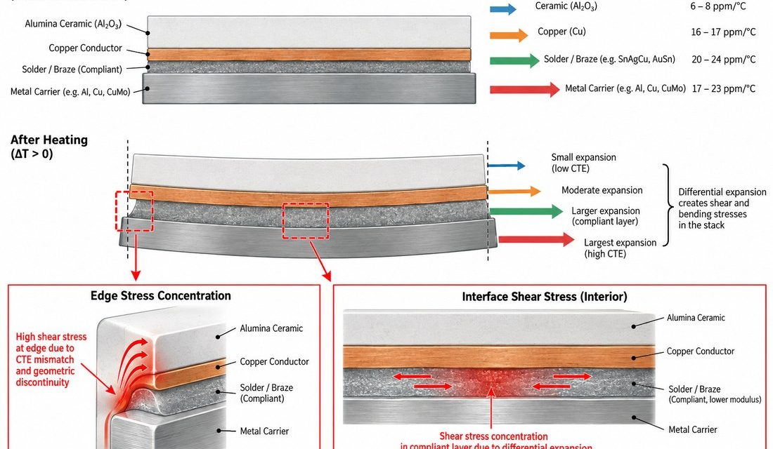
A high-power Alumina PCB can carry heat efficiently only when the copper, substrate, solder or braze, and metal carrier move together. Repeated temperature change makes the interface a mechanical system. The most common project mistake is to qualify the ceramic coupon while the product uses a different copper area, fastener pattern, or thermal interface. A...

Alumina PCB for mmWave Packaging: Cavity, Ground, and Connector Datum Control

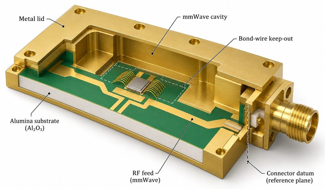
In a compact mmWave package, the Alumina PCB is often both circuit carrier and mechanical reference. A cavity, lid, bond window, connector, or waveguide transition can define the electromagnetic boundary more strongly than a long trace. The project risk is a datum mismatch: the electrical drawing references the board edge while the housing references the...

Alumina PCB Thick-Film RF Modules: Balancing Thermal Spreading and Layout Density

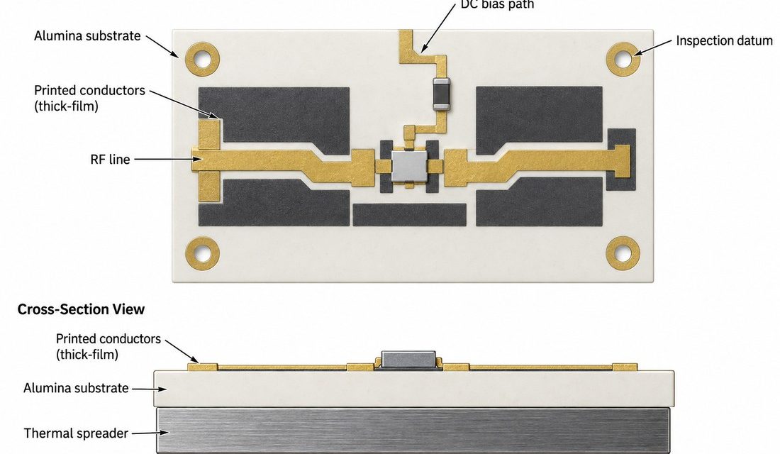
Alumina remains a practical ceramic substrate for RF modules, sensor hybrids, and compact power interfaces because it combines electrical insulation with a stable mechanical base. The challenge is density. A Alumina PCB can carry thick-film conductors, thin-film features, soldered parts, and a thermal interface in a small area, but every added pad or crossover changes...

PTFE PCB DFM: Panelization and Procurement Controls for Repeatable RF Builds

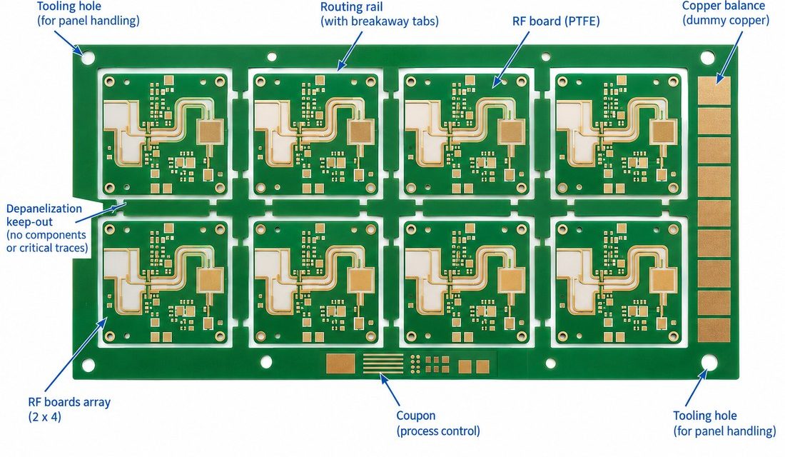
A PTFE board can be electrically well designed and still be difficult to quote or panelize. The manufacturing risk is concentrated at the interfaces: copper balance, drilled features, plated edges, hybrid stackup boundaries, connector rails, and the coupon that is supposed to represent the RF path. A PTFE PCB release should therefore explain the process...