HomeCategory

Customer Cases | PCB & PCBA Success Stories - KKPCB

Advantages and Disadvantages of Multilayer PCBs

With the continuous development of electronic products toward higher performance, smaller size, and greater functional integration, traditional single-layer and double-layer PCBs can no longer satisfy the requirements of many advanced applications. A multilayer PCB is a circuit board composed of multiple conductive copper layers laminated together with insulating dielectric materials. By increasing the number of...

Comprehensive Guide to IC Substrates and Their Role in Electronics

As semiconductor devices continue to evolve toward higher processing performance, smaller package sizes, and greater integration density, traditional PCB technologies alone are no longer sufficient to meet the interconnection requirements between silicon chips and electronic systems. IC substrates serve as a critical connection platform between semiconductor chips and printed circuit boards (PCBs), enabling reliable electrical...

Optimized Article: Multilayer FR4 PCB Substrate Material and Ceramic PCB Comparison

Material selection is one of the most important decisions in PCB development. As electronic products continue evolving toward higher power density, higher frequency operation, and increased reliability requirements, engineers must carefully evaluate whether traditional PCB materials or advanced substrate technologies are suitable for specific applications. Among various PCB substrate solutions, multilayer FR4 PCBs and ceramic...

Comprehensive Guide to RF PCB Design

With the rapid development of wireless communication, radar systems, IoT devices, automotive electronics, and satellite communication technologies, RF (Radio Frequency) PCB design has become increasingly important in modern electronic systems. Unlike conventional digital PCBs, RF PCBs operate at high frequencies where even small variations in: Material properties Trace geometry Layer structure Grounding design Manufacturing tolerance...

Annular Ring in PCB: Key Considerations for Design and Manufacturing

In PCB design and manufacturing, every detail of the circuit structure can influence the reliability and performance of the final product. Among these details, the annular ring is a critical but often overlooked factor that directly affects via reliability, electrical connectivity, and manufacturing yield. The annular ring refers to the copper area surrounding a drilled...

What to Look For When Choosing a Fast Flex PCB Manufacturer

As electronic products continue to evolve toward miniaturization, lightweight structures, and higher integration, flexible printed circuit boards (Flex PCBs) have become an essential technology for modern electronic systems. Compared with traditional rigid PCBs, Flex PCBs offer unique advantages: Three-dimensional assembly capability Reduced product thickness and weight Improved space utilization Fewer connectors and wiring components Better...

Copper Core PCB: A Revolution in the Electronics Industry

With the rapid development of high-power electronics, electric vehicles, LED lighting, renewable energy systems, and advanced industrial equipment, thermal management has become one of the most critical challenges in electronic product design. As electronic components become more compact while power density continues to increase, traditional FR-4 PCBs may face limitations in heat dissipation performance. Copper...

Semi-Rigid PCBs: The Future of Compact and Durable Electronics

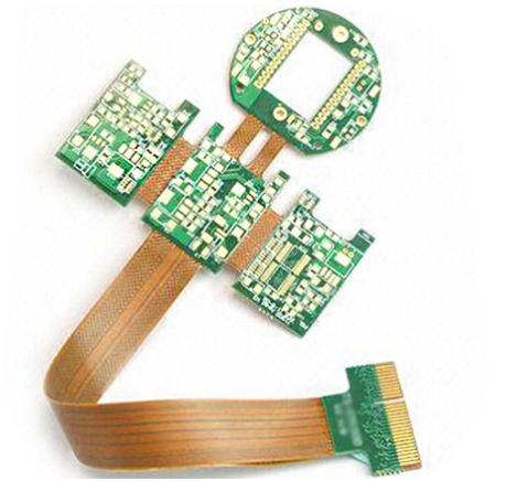
With the continuous evolution of electronic products toward miniaturization, lightweight design, and higher reliability, traditional rigid PCBs and flexible PCBs each face certain limitations in advanced applications. Rigid PCBs provide excellent mechanical strength and dimensional stability but lack flexibility for complex installation environments. Flexible PCBs offer excellent bending capability and space utilization but may not...

HDI PCB Design: Comprehensive Guidelines, Processes, and Considerations

With electronic products continuing to evolve toward smaller dimensions, higher functionality, and faster signal transmission, traditional PCB technologies are increasingly challenged by limitations in routing density and component integration. High Density Interconnect (HDI) PCB technology provides an effective solution by using advanced interconnection structures such as: Microvias Blind vias Buried vias Fine-line traces High-density layer...

What is Backdrill and How Was It Done in PCB Manufacturing?

As electronic products continue to demand higher data rates, faster signal transmission, and improved signal integrity, traditional PCB manufacturing methods face increasing challenges. In high-speed PCB designs, even small parasitic effects caused by vias can negatively impact signal performance. One common issue is the via stub, which is the unused portion of a plated through...