
As electronic products continue to demand higher data rates, faster signal transmission, and improved signal integrity, traditional PCB manufacturing methods face increasing challenges. In high-speed PCB designs, even small parasitic effects caused by vias can negatively impact signal performance.
One common issue is the via stub, which is the unused portion of a plated through hole extending beyond the layer where the signal exits. At high frequencies, these unused via sections can behave like transmission line stubs, causing:
- Signal reflection
- Resonance
- Insertion loss
- Timing distortion
To solve this problem, PCB manufacturers use a specialized process called backdrilling (also known as controlled-depth drilling).
Backdrilling removes the unnecessary portion of a through-hole via after the main drilling and plating process, reducing signal interference and improving high-speed transmission performance.
1. What Is Backdrill in PCB Manufacturing?
1.1 Definition of Backdrilling
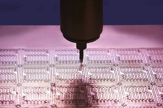
Backdrilling is a PCB manufacturing process that removes the unused copper barrel section of a plated through hole (PTH) from the opposite side of the PCB.
During normal PCB fabrication, a through via extends through the entire board thickness. However, many high-speed signals only need to connect between specific layers.
The remaining unused via section becomes a via stub.
Backdrilling removes this unwanted section while leaving the required electrical connection intact.
1.2 Structure of a Normal Via Without Backdrill
A conventional through-hole via passes through all PCB layers.
For example:
- Signal enters from Layer 1
- Connects to Layer 6
- Via continues down to Layer 12
The unused portion from Layer 7 to Layer 12 is the via stub.
At low frequencies, this stub may have little impact.
However, at high frequencies, it can create impedance discontinuities.
1.3 Structure After Backdrilling
After backdrilling:
- The required signal connection remains.
- The unnecessary via barrel is removed.
- The remaining stub length is minimized.
This improves high-speed electrical performance.
2. Why Is Backdrilling Needed?
2.1 Reduce Signal Reflection
A via stub creates an impedance discontinuity.
When high-speed signals encounter this discontinuity, part of the signal energy reflects back.
Possible effects include:
- Eye diagram degradation
- Increased jitter
- Data transmission errors
Backdrilling reduces these reflections by removing unnecessary via sections.
2.2 Improve Signal Integrity
High-speed interfaces are sensitive to small electrical variations.
Backdrilling helps improve:
- Signal waveform quality
- Transmission stability
- Timing accuracy
It is commonly used for:
- High-speed serial interfaces
- Differential signals
- RF-related connections
2.3 Reduce Resonance Effects
A via stub can act as a small antenna or resonant structure.
At certain frequencies, it may cause:
- Noise amplification
- Signal attenuation
- Electromagnetic interference
Removing the stub reduces these unwanted effects.
3. Applications Requiring Backdrill Technology
Backdrilling is mainly used in high-speed and high-frequency PCB applications.
3.1 High-Speed Communication Equipment
Examples:
- Network switches
- Routers
- Data transmission equipment
High-speed channels require excellent signal integrity.
3.2 Server and Computing Systems
Applications include:
- AI servers
- Data centers
- High-performance computing platforms
Interfaces such as:
- PCIe
- High-speed memory buses
often require optimized via structures.
3.3 5G and RF Communication Equipment
RF and microwave signals are highly sensitive to parasitic effects.
Backdrilling helps reduce:
- Signal loss
- Reflection
- Phase distortion
3.4 Semiconductor Test Equipment
ATE (Automatic Test Equipment) and load boards require extremely stable high-speed connections.
Backdrilling helps improve:
- Test signal accuracy
- Measurement repeatability
- High-frequency performance
4. Backdrilling Process in PCB Manufacturing
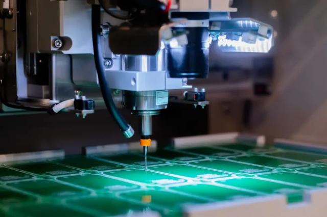
The backdrilling process is performed after standard PCB drilling and plating.
The typical manufacturing sequence includes:
Step 1: PCB Layer Stackup Design
Before production, engineers determine:
- Signal layer connections
- Via structures
- Required drilling depth
The stackup must define:
- Start layer
- Target layer
- Backdrill depth
Accurate stackup information is essential for successful processing.
Step 2: Standard Via Drilling
The PCB undergoes normal mechanical drilling.
The holes are drilled through the entire board thickness.
Step 3: Copper Plating
After drilling:
- Hole walls are plated with copper.
- Electrical connections between layers are created.
At this stage, the via barrel extends through the full PCB.
Step 4: Backdrill Data Generation
Manufacturing engineers generate special drilling files based on:
- Gerber data
- ODB++ data
- Stackup information
The file defines:
- Backdrill location
- Drill diameter
- Drilling depth
- Remaining stub length
Step 5: Controlled-Depth Backdrilling
A larger drill bit removes the unwanted via barrel from the opposite side.
The drilling depth is carefully controlled to stop before reaching the active signal layer.
Important parameters include:
- Drill depth tolerance
- Tool accuracy
- Remaining copper length
Step 6: Inspection and Verification
After backdrilling, manufacturers verify:
- Hole depth
- Remaining stub length
- Electrical continuity
- Mechanical accuracy
Inspection methods may include:
- Cross-section analysis
- X-ray inspection
- Electrical testing
5. Key Design Considerations for Backdrilling
5.1 Stackup Accuracy
Backdrilling depends heavily on accurate layer thickness information.
Errors in:
- Dielectric thickness
- Copper thickness
- Lamination variation
can affect drilling depth.
5.2 Remaining Stub Length
The goal is to minimize the remaining via stub.
However, completely removing all copper is not always necessary.
Manufacturers typically maintain a controlled residual length based on:
- Signal frequency
- Design requirements
- Manufacturing tolerance
5.3 Drill Diameter Selection
The backdrill diameter must be larger than the original via diameter.
Considerations include:
- Clearance from surrounding traces
- Pad size
- Manufacturing capability
5.4 PCB Thickness
Thicker PCBs usually have longer via stubs, making backdrilling more valuable.
Applications involving:
- 10-layer+
- 12-layer+
- 16-layer+ PCBs
often benefit from this technology.
6. Advantages and Limitations of Backdrilling
Advantages
Improved Signal Integrity
Reduces:
- Reflection
- Signal distortion
- Transmission loss
Better High-Speed Performance
Supports:
- Higher data rates
- More reliable communication
Reduced EMI Problems
Minimizes unwanted radiation caused by via resonance.
Limitations
Increased Manufacturing Cost
Additional processing requires:
- Extra drilling operations
- More inspection procedures
- Advanced manufacturing equipment
More Complex Manufacturing Control
Requires:
- Precise depth control
- Accurate stackup information
- Experienced PCB manufacturers
Not Required for Every PCB
Low-speed circuits usually do not need backdrilling.
It is mainly beneficial when:
- Signal frequency is high
- Data rate is high
- Via stubs affect performance
7. Backdrill vs Blind Via vs Buried Via
| Technology | Description | Main Advantage |
|---|---|---|
| Through Via | Hole passes through entire PCB | Low cost and simple |
| Blind Via | Connects outer layer to internal layer | Saves routing space |
| Buried Via | Connects internal layers only | Improves density |
| Backdrill | Removes unused via section | Improves high-speed signal integrity |
8. Backdrilling and DFM Considerations
Because backdrilling requires precise manufacturing control, early DFM review is important.
Engineers should evaluate:
- Stackup feasibility
- Drill tolerance
- Via arrangement
- Layer transitions
- Manufacturing capability
A PCB manufacturer should confirm:
- Maximum backdrill depth
- Minimum remaining stub requirement
- Drill accuracy capability
before production begins.
Conclusion
Backdrilling is an advanced PCB manufacturing technology designed to improve high-speed signal performance by removing unnecessary via stubs from plated through holes.
By reducing:
- Signal reflections
- Resonance effects
- Impedance discontinuities
backdrilling helps achieve better signal integrity in applications such as:
- High-speed communication systems
- Servers
- 5G equipment
- Semiconductor test boards
- Advanced industrial electronics
Although it increases manufacturing complexity and cost, backdrilling becomes increasingly valuable as PCB designs move toward higher frequencies and faster data transmission speeds.
Through proper stackup planning, accurate drilling control, and DFM collaboration between designers and manufacturers, backdrill technology enables more reliable and high-performance PCB solutions.
