
With electronic products continuing to evolve toward smaller dimensions, higher functionality, and faster signal transmission, traditional PCB technologies are increasingly challenged by limitations in routing density and component integration.
High Density Interconnect (HDI) PCB technology provides an effective solution by using advanced interconnection structures such as:
- Microvias
- Blind vias
- Buried vias
- Fine-line traces
- High-density layer stacking
HDI PCBs enable designers to achieve:
- Higher wiring density
- Smaller PCB size
- Improved electrical performance
- More compact electronic systems
They are widely used in advanced applications including:
- Smartphones
- Wearable devices
- Automotive electronics
- Medical equipment
- Semiconductor test systems
- High-speed communication products
This article introduces HDI PCB design principles, manufacturing processes, key design guidelines, and important considerations for reliable production.
1. What Is an HDI PCB?
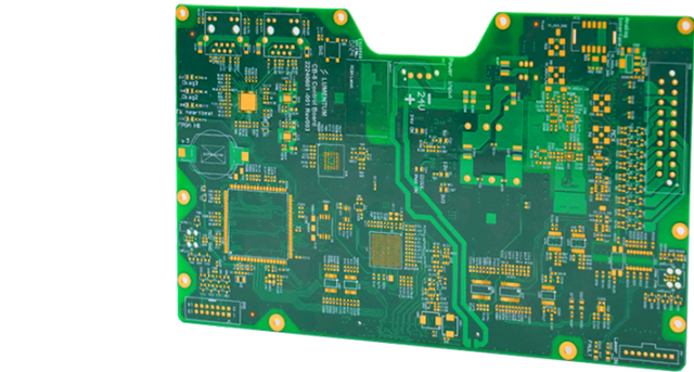
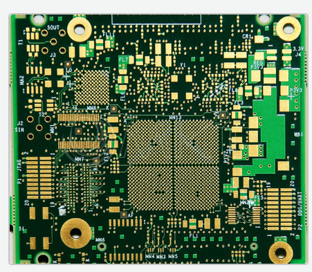
HDI (High Density Interconnect) PCB is an advanced printed circuit board technology designed to achieve higher interconnection density compared with conventional multilayer PCBs.
The main difference between HDI PCBs and traditional PCBs is the use of microvia technology.
Microvias are very small laser-drilled holes that connect adjacent PCB layers, allowing designers to create more compact routing structures.
Key Features of HDI PCB
HDI PCBs typically include:
- Smaller via structures
- Finer trace width and spacing
- Higher layer interconnection density
- More compact component placement
Compared with conventional vias, microvias provide:
- Shorter electrical paths
- Reduced parasitic effects
- Improved signal performance
2. Why HDI PCB Technology Is Important
2.1 Miniaturization of Electronic Products
Modern products require more functions in smaller spaces.
HDI technology allows:
- Smaller PCB dimensions
- More components per unit area
- Reduced system size
Applications include:
- Smartphones
- Wearable electronics
- Portable medical devices
2.2 Improved Signal Integrity
As signal speeds increase, transmission quality becomes more important.
HDI structures help improve:
- Signal path length
- Impedance control
- High-speed transmission performance
Benefits include:
- Reduced signal loss
- Lower parasitic capacitance
- Better high-frequency performance
2.3 Higher Component Density
HDI PCBs support advanced packages such as:
- BGA
- CSP
- Fine-pitch IC packages
They provide better routing capability under high-density components.
3. HDI PCB Via Structures
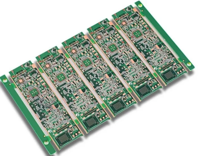
The via structure is one of the most important aspects of HDI PCB design.
3.1 Microvia
A microvia is a small-diameter via created using laser drilling technology.
Characteristics:
- Small hole size
- High-density connection capability
- Short signal path
Applications:
- Fine-pitch components
- Advanced multilayer PCBs
3.2 Blind Via
A blind via connects:
- Outer layer to internal layer
but does not pass through the entire PCB.
Advantages:
- Saves routing space
- Improves layer utilization
3.3 Buried Via
A buried via connects internal layers only.
Advantages:
- Further increases routing density
- Allows more compact designs
3.4 Stacked and Staggered Microvias
Stacked Microvias
Microvias are vertically aligned.
Advantages:
- Maximum density
- Suitable for advanced HDI designs
Challenges:
- More complex manufacturing
- Higher process control requirements
Staggered Microvias
Microvias are offset between layers.
Advantages:
- Better manufacturing reliability
- Lower process complexity
4. HDI PCB Manufacturing Process
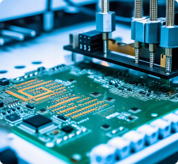
HDI PCB manufacturing requires advanced fabrication processes.
4.1 Inner Layer Fabrication
The process begins with inner layer circuit formation.
Steps include:
- Copper preparation
- Photo imaging
- Etching
- AOI inspection
Precision control is required for:
- Fine traces
- Layer alignment
4.2 Lamination
Multiple PCB layers are bonded together through lamination.
Important parameters include:
- Temperature
- Pressure
- Resin flow
Poor lamination may cause:
- Delamination
- Layer misalignment
4.3 Laser Drilling Microvias
Laser drilling creates microvias for layer connections.
Advantages:
- High precision
- Small hole size
- Suitable for fine-density designs
Process control affects:
- Hole quality
- Copper plating reliability
4.4 Copper Plating
Copper plating forms conductive connections inside microvias.
Important factors:
- Copper thickness
- Filling quality
- Plating uniformity
Poor plating may lead to:
- Via cracks
- Open circuits
4.5 Sequential Lamination
Many HDI PCBs require multiple lamination cycles.
This process enables:
- More complex layer structures
- Advanced via combinations
Examples:
- 1+N+1 HDI
- 2+N+2 HDI
- Any-layer HDI
5. HDI PCB Stack-Up Types
5.1 1+N+1 HDI
Structure:
- One HDI build-up layer on each side
- Conventional core layers inside
Advantages:
- Cost-effective
- Suitable for many applications
5.2 2+N+2 HDI
Structure:
- Two build-up layers on each side
Advantages:
- Higher routing density
- Suitable for complex designs
Applications:
- Advanced computing
- Communication equipment
5.3 Any-Layer HDI
Any-layer HDI allows microvias to connect any layer.
Advantages:
- Maximum design flexibility
- Extremely high density
Applications:
- Smartphones
- Advanced semiconductor systems
6. HDI PCB Design Guidelines
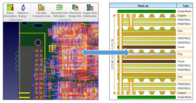
6.1 Layer Stack-Up Design
A proper stack-up is critical for:
- Signal integrity
- Manufacturing reliability
- Cost control
Design considerations include:
- Signal layer arrangement
- Ground plane distribution
- Dielectric thickness
- Impedance requirements
6.2 Trace Width and Spacing
HDI designs typically require finer traces.
Important considerations:
- Manufacturing capability
- Copper thickness
- Signal requirements
Fine-line design improves:
- Routing density
- Component integration
6.3 Microvia Design Rules
Engineers should consider:
- Via diameter
- Via depth
- Aspect ratio
- Pad size
Poor microvia design may cause:
- Via failure
- Manufacturing defects
6.4 BGA Fan-Out Design
HDI technology is commonly used for BGA routing.
Design methods include:
- Via-in-pad
- Microvia fan-out
- Escape routing optimization
Benefits:
- Reduced PCB size
- Improved routing efficiency
6.5 Impedance Control
High-speed HDI PCBs require controlled impedance.
Factors affecting impedance include:
- Trace width
- Copper thickness
- Dielectric thickness
- Material properties
Applications requiring impedance control include:
- High-speed processors
- RF modules
- Communication systems
7. Key Manufacturing Considerations for HDI PCB
7.1 Via Reliability
Microvias experience thermal and mechanical stress.
Potential failures:
- Copper cracking
- Interface separation
- Pad failure
Reliability depends on:
- Material selection
- Copper plating quality
- Manufacturing process control
7.2 Layer Alignment Accuracy
HDI requires precise registration between layers.
Poor alignment may cause:
- Open circuits
- Connection failures
7.3 Material Selection
Common materials include:
High-Tg FR-4
Advantages:
- Good thermal stability
- Cost-effective
Low-Loss Materials
Used for:
- High-speed applications
- RF circuits
Requirements:
- Stable Dk
- Low signal loss
8. HDI PCB Reliability Testing
Advanced HDI PCBs require strict testing.
Electrical Testing
Includes:
- Continuity testing
- Insulation testing
- Impedance testing
AOI Inspection
Detects:
- Pattern defects
- Missing circuits
- Alignment issues
X-Ray Inspection
Used for:
- Microvia inspection
- Hidden structure analysis
Thermal Cycling Testing
Evaluates:
- Via reliability
- Material stability
9. Applications of HDI PCBs
Consumer Electronics
Examples:
- Smartphones
- Tablets
- Smart watches
Requirements:
- Small size
- High integration
Automotive Electronics
Applications:
- ADAS systems
- Vehicle control units
- Sensor modules
Requirements:
- Reliability
- Signal performance
Medical Devices
Applications:
- Portable diagnostic equipment
- Monitoring devices
Requirements:
- Compact design
- High reliability
Semiconductor Equipment
Applications:
- ATE load boards
- Test interface boards
Requirements:
- High-density routing
- Precise electrical performance
Communication Equipment
Applications:
- Network equipment
- 5G systems
Requirements:
- High-speed signal transmission
- Controlled impedance
10. Advantages and Limitations of HDI PCB
Advantages
- Higher wiring density
- Smaller PCB size
- Better signal integrity
- Supports advanced IC packages
- Improved electrical performance
Limitations
- Higher manufacturing cost
- More complex fabrication process
- Requires advanced production capability
- Higher process control requirements
Conclusion
HDI PCB technology has become an essential solution for modern electronic products requiring high density, miniaturization, and high-speed performance.
Successful HDI PCB development requires careful consideration of:
- Stack-up design
- Microvia structures
- Material selection
- Impedance control
- Manufacturing capability
- Reliability testing
With the continued growth of applications such as 5G communication, automotive electronics, semiconductor testing, and advanced consumer devices, HDI PCBs will continue to play a key role in next-generation electronic system development.
